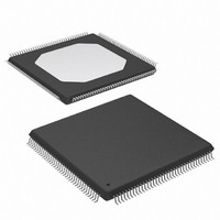
XC3S250E-4TQG144C Xilinx Inc, XC3S250E-4TQG144C Datasheet - Page 41

XC3S250E-4TQG144C
Manufacturer Part Number
XC3S250E-4TQG144C
Description
IC SPARTAN-3E FPGA 250K 144TQFP
Manufacturer
Xilinx Inc
Series
Spartan™-3Er
Datasheet
1.XC3S100E-4VQG100C.pdf
(233 pages)
Specifications of XC3S250E-4TQG144C
Number Of Logic Elements/cells
5508
Number Of Labs/clbs
612
Total Ram Bits
221184
Number Of I /o
108
Number Of Gates
250000
Voltage - Supply
1.14 V ~ 1.26 V
Mounting Type
Surface Mount
Operating Temperature
0°C ~ 85°C
Package / Case
144-LQFP
For Use With
813-1009 - MODULE USB-TO-FPGA TOOL W/MANUAL
Lead Free Status / RoHS Status
Lead free / RoHS Compliant
Other names
122-1524
Available stocks
Company
Part Number
Manufacturer
Quantity
Price
Company:
Part Number:
XC3S250E-4TQG144C
Manufacturer:
XILINX
Quantity:
2 000
Company:
Part Number:
XC3S250E-4TQG144C
Manufacturer:
XILINX
Quantity:
2 400
Company:
Part Number:
XC3S250E-4TQG144C
Manufacturer:
Xilinx Inc
Quantity:
10 000
Part Number:
XC3S250E-4TQG144C
Manufacturer:
XILINX/赛灵思
Quantity:
20 000
Part Number:
XC3S250E-4TQG144CS1
Manufacturer:
XILINX/赛灵思
Quantity:
20 000
Table 25: Block RAM Function Table (Continued)
There are a number of different conditions under which data
can be accessed at the DO outputs. Basic data access
always occurs when the WE input is inactive. Under this
condition, data stored in the memory location addressed by
the ADDR lines passes through a output latch to the DO
outputs. The timing for basic data access is shown in the
Table 26: WRITE_MODE Effect on Data Output Latches During Write Operations
DS312-2 (v3.8) August 26, 2009
Product Specification
GSR
WRITE_FIRST
Read After Write
READ_FIRST
Read Before Write
NO_CHANGE
No Read on Write
0
Write Mode
EN
1
R
SSR
0
Input Signals
WE
Data on DI and DIP inputs is written into
specified RAM location and simultaneously
appears on DO and DOP outputs.
Data from specified RAM location appears on
DO and DOP outputs.
Data on DI and DIP inputs is written into
specified location.
Data on DO and DOP outputs remains
unchanged.
Data on DI and DIP inputs is written into
specified location.
1
CLK
↑
Effect on Same Port
ADDR
Write RAM, Simultaneous Read Operation
addr
pdata
DIP
www.xilinx.com
Data
DI
RAM(data)
portions of
which WE is Low.
Data also can be accessed on the DO outputs when assert-
ing the WE input based on the value of the
attribute as described in
No Chg
pdata
DOP
Output Signals
Invalidates data on DO and DOP outputs.
Data from specified RAM location appears on
DO and DOP outputs.
Invalidates data on DO and DOP outputs.
WRITE_MODE = WRITE_FIRST
WRITE_MODE = NO_CHANGE
WRITE_MODE = READ_FIRST
Figure
RAM(data)
(dual-port only with same address)
No Chg
data
DO
33,
Effect on Opposite Port
Table
Figure
RAM(addr)
RAM(addr)
RAM(addr)
26.
← pdata
← pdata
← pdata
34, and
Parity
Functional Description
RAM Data
Figure 35
WRITE_MODE
RAM(addr)
RAM(addr)
RAM(addr)
← pdata
← pdata
← data
Data
during
41


