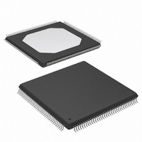
XC3S250E-4TQG144C Xilinx Inc, XC3S250E-4TQG144C Datasheet - Page 136

XC3S250E-4TQG144C
Manufacturer Part Number
XC3S250E-4TQG144C
Description
IC SPARTAN-3E FPGA 250K 144TQFP
Manufacturer
Xilinx Inc
Series
Spartan™-3Er
Datasheet
1.XC3S100E-4VQG100C.pdf
(233 pages)
Specifications of XC3S250E-4TQG144C
Number Of Logic Elements/cells
5508
Number Of Labs/clbs
612
Total Ram Bits
221184
Number Of I /o
108
Number Of Gates
250000
Voltage - Supply
1.14 V ~ 1.26 V
Mounting Type
Surface Mount
Operating Temperature
0°C ~ 85°C
Package / Case
144-LQFP
For Use With
813-1009 - MODULE USB-TO-FPGA TOOL W/MANUAL
Lead Free Status / RoHS Status
Lead free / RoHS Compliant
Other names
122-1524
Available stocks
Company
Part Number
Manufacturer
Quantity
Price
Company:
Part Number:
XC3S250E-4TQG144C
Manufacturer:
XILINX
Quantity:
2 000
Company:
Part Number:
XC3S250E-4TQG144C
Manufacturer:
XILINX
Quantity:
2 400
Company:
Part Number:
XC3S250E-4TQG144C
Manufacturer:
Xilinx Inc
Quantity:
10 000
Part Number:
XC3S250E-4TQG144C
Manufacturer:
XILINX/赛灵思
Quantity:
20 000
Part Number:
XC3S250E-4TQG144CS1
Manufacturer:
XILINX/赛灵思
Quantity:
20 000
DC and Switching Characteristics
Simultaneously Switching Output Guidelines
This section provides guidelines for the recommended max-
imum allowable number of Simultaneous Switching Outputs
(SSOs). These guidelines describe the maximum number
of user I/O pins of a given output signal standard that should
simultaneously switch in the same direction, while maintain-
ing a safe level of switching noise. Meeting these guidelines
for the stated test conditions ensures that the FPGA oper-
ates free from the adverse effects of ground and power
bounce.
Ground or power bounce occurs when a large number of
outputs simultaneously switch in the same direction. The
output drive transistors all conduct current to a common
voltage rail. Low-to-High transitions conduct to the V
rail; High-to-Low transitions conduct to the GND rail. The
resulting cumulative current transient induces a voltage dif-
ference across the inductance that exists between the die
pad and the power supply or ground return. The inductance
is associated with bonding wires, the package lead frame,
and any other signal routing inside the package. Other vari-
ables contribute to SSO noise levels, including stray induc-
tance on the PCB as well as capacitive loading at receivers.
Any SSO-induced voltage consequently affects internal
switching noise margins and ultimately signal quality.
Table 96
lines. For each device/package combination,
vides the number of equivalent V
Table 96: Equivalent V
136
XC3S100E
XC3S250E
XC3S500E
XC3S1200E
XC3S1600E
Device
and
Table 97
VQ100
2
2
2
-
-
provide the essential SSO guide-
CCO
/GND Pairs per Bank
CP132
2
2
2
-
-
CCO
/GND pairs. The
Table 96
TQ144
2
2
-
-
-
Package Style (including Pb-free)
www.xilinx.com
CCO
pro-
PQ208
equivalent number of pairs is based on characterization and
might not match the physical number of pairs. For each out-
put signal standard and drive strength,
mends the maximum number of SSOs, switching in the
same direction, allowed per V
bank. The guidelines in
age style. Multiply the appropriate numbers from
and
allowed within an I/O bank. Exceeding these SSO guide-
lines might result in increased power or ground bounce,
degraded signal integrity, or increased system jitter.
The recommended maximum SSO values assumes that the
FPGA is soldered on the printed circuit board and that the
board uses sound design practices. The SSO values do not
apply for FPGAs mounted in sockets, due to the lead induc-
tance introduced by the socket.
The number of SSOs allowed for quad-flat packages (VQ,
TQ, PQ) is lower than for ball grid array packages (FG) due
to the larger lead inductance of the quad-flat packages. The
results for chip-scale packaging (CP132) are better than
quad-flat packaging but not as high as for ball grid array
packaging. Ball grid array packages are recommended for
applications with a large number of simultaneously switch-
ing outputs.
3
3
-
-
-
SSO
Table 97
MAX
FT256
/IO Bank =
4
4
4
-
-
to calculate the maximum number of SSOs
FG320
Table 96
Table 97
5
5
5
-
-
DS312-3 (v3.8) August 26, 2009
CCO
x
are categorized by pack-
/GND pair within an I/O
Table 97
FG400
Product Specification
6
6
-
-
-
Table 97
FG484
Table 96
recom-
7
-
-
-
-
R


