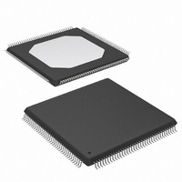
XC3S250E-4TQG144C Xilinx Inc, XC3S250E-4TQG144C Datasheet - Page 159

XC3S250E-4TQG144C
Manufacturer Part Number
XC3S250E-4TQG144C
Description
IC SPARTAN-3E FPGA 250K 144TQFP
Manufacturer
Xilinx Inc
Series
Spartan™-3Er
Datasheet
1.XC3S100E-4VQG100C.pdf
(233 pages)
Specifications of XC3S250E-4TQG144C
Number Of Logic Elements/cells
5508
Number Of Labs/clbs
612
Total Ram Bits
221184
Number Of I /o
108
Number Of Gates
250000
Voltage - Supply
1.14 V ~ 1.26 V
Mounting Type
Surface Mount
Operating Temperature
0°C ~ 85°C
Package / Case
144-LQFP
For Use With
813-1009 - MODULE USB-TO-FPGA TOOL W/MANUAL
Lead Free Status / RoHS Status
Lead free / RoHS Compliant
Other names
122-1524
Available stocks
Company
Part Number
Manufacturer
Quantity
Price
Company:
Part Number:
XC3S250E-4TQG144C
Manufacturer:
XILINX
Quantity:
2 000
Company:
Part Number:
XC3S250E-4TQG144C
Manufacturer:
XILINX
Quantity:
2 400
Company:
Part Number:
XC3S250E-4TQG144C
Manufacturer:
Xilinx Inc
Quantity:
10 000
Part Number:
XC3S250E-4TQG144C
Manufacturer:
XILINX/赛灵思
Quantity:
20 000
Part Number:
XC3S250E-4TQG144CS1
Manufacturer:
XILINX/赛灵思
Quantity:
20 000
Table 121: Configuration Timing Requirements for Attached Parallel NOR Flash
Table 122: MultiBoot Trigger (MBT) Timing
DS312-3 (v3.8) August 26, 2009
Product Specification
Notes:
1.
2.
3.
Notes:
1.
T
(t
T
(t
T
(t
T
(t
Symbol
ACC
OE
CE
ELQV
GLQV
AVQV
BYTE
FLQV,
Symbol
T
These requirements are for successful FPGA configuration in BPI mode, where the FPGA provides the CCLK frequency. The post
configuration timing can be different to support the specific needs of the application loaded into the FPGA and the resulting clock source.
Subtract additional printed circuit board routing delay as required by the application.
The initial BYTE# timing can be extended using an external, appropriately sized pull-down resistor on the FPGA’s LDC2 pin. The resistor
value also depends on whether the FPGA’s HSWAP pin is High or Low.
MultiBoot re-configuration starts on the rising edge after MBT is Low for at least the prescribed minimum period.
MBT
)
)
)
t
FHQV
R
)
MultiBoot Trigger (MBT) Low pulse width required to initiate
MultiBoot reconfiguration
Parallel NOR Flash PROM chip-select
time
Parallel NOR Flash PROM
output-enable time
Parallel NOR Flash PROM read access
time
For x8/x16 PROMs only: BYTE# to
output valid time
Description
(3)
Description
www.xilinx.com
T
ACC
≤
0.5T
CCLKn min
T
T
T
BYTE
CE
OE
Requirement
(
≤
≤
≤
T
Minimum
T
)
T
DC and Switching Characteristics
INITADDR
INITADDR
–
300
INITADDR
T
CCO
–
T
DCC
Maximum
–
∞
PCB
Units
Units
ns
ns
ns
ns
ns
159


