MC9S12NE64CPV Freescale Semiconductor, MC9S12NE64CPV Datasheet - Page 420
MC9S12NE64CPV
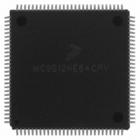
Manufacturer Part Number
MC9S12NE64CPV
Description
IC MCU 25MHZ ETHERNT/PHY 112LQFP
Manufacturer
Freescale Semiconductor
Series
HCS12r
Datasheet
1.MC9S12NE64VTU.pdf
(554 pages)
Specifications of MC9S12NE64CPV
Mfg Application Notes
MC9S12NE64 Integrated Ethernet Controller Implementing an Ethernet Interface with the MC9S12NE64 Web Server Development with MC9S12NE64 and Open TCP
Core Processor
HCS12
Core Size
16-Bit
Speed
25MHz
Connectivity
EBI/EMI, Ethernet, I²C, SCI, SPI
Peripherals
POR, PWM, WDT
Number Of I /o
70
Program Memory Size
64KB (64K x 8)
Program Memory Type
FLASH
Ram Size
8K x 8
Voltage - Supply (vcc/vdd)
2.375 V ~ 3.465 V
Data Converters
A/D 8x10b
Oscillator Type
Internal
Operating Temperature
-40°C ~ 85°C
Package / Case
112-LQFP
Data Bus Width
16 bit
Data Ram Size
8 KB
Interface Type
I2C, SCI, SPI
Maximum Clock Frequency
25 MHz
Number Of Programmable I/os
70
Number Of Timers
16 bit
Operating Supply Voltage
- 0.3 V to + 3 V
Maximum Operating Temperature
+ 105 C
Mounting Style
SMD/SMT
Minimum Operating Temperature
- 65 C
On-chip Adc
10 bit
For Use With
EVB9S12NE64E - BOARD EVAL FOR 9S12NE64DEMO9S12NE64E - DEMO BOARD FOR 9S12NE64
Lead Free Status / RoHS Status
Contains lead / RoHS non-compliant
Eeprom Size
-
Lead Free Status / Rohs Status
No RoHS Version Available
Available stocks
Company
Part Number
Manufacturer
Quantity
Price
Company:

Part Number:
MC9S12NE64CPV
Manufacturer:
RENESAS
Quantity:
21 000
Company:
Part Number:
MC9S12NE64CPV
Manufacturer:
FREESCAL
Quantity:
455
Company:
Part Number:
MC9S12NE64CPV
Manufacturer:
Freescale Semiconductor
Quantity:
10 000
Company:
Part Number:
MC9S12NE64CPVE
Manufacturer:
ST
Quantity:
445
Company:
Part Number:
MC9S12NE64CPVE
Manufacturer:
Freescale Semiconductor
Quantity:
10 000


Chapter 15 Multiplexed External Bus Interface (MEBIV3)
The PE4/ECLK pin is initially configured as ECLK output with stretch. The E clock output function
depends upon the settings of the NECLK bit in the PEAR register, the IVIS bit in the MODE register and
the ESTR bit in the EBICTL register. In normal expanded narrow mode, the E clock is available for use in
external select decode logic or as a constant speed clock for use in the external application system.
The PE2/R/W pin is initially configured as a general purpose input with an internal pull resistor enabled
but this pin can be reconfigured as the R/W bus control signal by writing “1” to the RDWE bit in PEAR.
If the expanded narrow system includes external devices that can be written such as RAM, the RDWE bit
would need to be set before any attempt to write to an external location. If there are no writable resources
in the external system, PE2 can be left as a general purpose I/O pin.
15.4.3.1.4
In expanded wide modes, Ports A and B are configured as a 16-bit multiplexed address and data bus and
Port E provides bus control and status signals. These signals allow external memory and peripheral devices
to be interfaced to the MCU. These signals can also be used by a logic analyzer to monitor the progress of
application programs.
The bus control related pins in Port E (PE7/NOACC, PE6/MODB/IPIPE1, PE5/MODA/IPIPE0,
PE4/ECLK, PE3/LSTRB/TAGLO, and PE2/R/W) are all configured to serve their bus control output
functions rather than general purpose I/O. Notice that writes to the bus control enable bits in the PEAR
register in emulation mode are restricted.
15.4.3.1.5
Expanded narrow modes are intended to allow connection of single 8-bit external memory devices for
lower cost systems that do not need the performance of a full 16-bit external data bus. Accesses to internal
resources that have been mapped external (i.e. PORTA, PORTB, DDRA, DDRB, PORTE, DDRE, PEAR,
PUCR, RDRIV) will be accessed with a 16-bit data bus on Ports A and B. Accesses of 16-bit external
words to addresses which are normally mapped external will be broken into two separate 8-bit accesses
using Port A as an 8-bit data bus. Internal operations continue to use full 16-bit data paths. They are only
visible externally as 16-bit information if IVIS=1.
Ports A and B are configured as multiplexed address and data output ports. During external accesses,
address A15, data D15 and D7 are associated with PA7, address A0 is associated with PB0 and data D8
and D0 are associated with PA0. During internal visible accesses and accesses to internal resources that
have been mapped external, address A15 and data D15 is associated with PA7 and address A0 and data
D0 is associated with PB0.
The bus control related pins in Port E (PE7/NOACC, PE6/MODB/IPIPE1, PE5/MODA/IPIPE0,
PE4/ECLK, PE3/LSTRB/TAGLO, and PE2/R/W) are all configured to serve their bus control output
functions rather than general purpose I/O. Notice that writes to the bus control enable bits in the PEAR
register in emulation mode are restricted.
The main difference between special modes and normal modes is that some of the bus control and system
control signals cannot be written in emulation modes.
420
Emulation Expanded Wide Mode
Emulation Expanded Narrow Mode
MC9S12NE64 Data Sheet, Rev. 1.1
Freescale Semiconductor
Related parts for MC9S12NE64CPV
Image
Part Number
Description
Manufacturer
Datasheet
Request
R

Part Number:
Description:
Manufacturer:
Freescale Semiconductor, Inc
Datasheet:
Part Number:
Description:
Manufacturer:
Freescale Semiconductor, Inc
Datasheet:
Part Number:
Description:
Manufacturer:
Freescale Semiconductor, Inc
Datasheet:
Part Number:
Description:
Manufacturer:
Freescale Semiconductor, Inc
Datasheet:
Part Number:
Description:
Manufacturer:
Freescale Semiconductor, Inc
Datasheet:
Part Number:
Description:
Manufacturer:
Freescale Semiconductor, Inc
Datasheet:
Part Number:
Description:
Manufacturer:
Freescale Semiconductor, Inc
Datasheet:
Part Number:
Description:
Manufacturer:
Freescale Semiconductor, Inc
Datasheet:
Part Number:
Description:
Manufacturer:
Freescale Semiconductor, Inc
Datasheet:
Part Number:
Description:
Manufacturer:
Freescale Semiconductor, Inc
Datasheet:
Part Number:
Description:
Manufacturer:
Freescale Semiconductor, Inc
Datasheet:
Part Number:
Description:
Manufacturer:
Freescale Semiconductor, Inc
Datasheet:
Part Number:
Description:
Manufacturer:
Freescale Semiconductor, Inc
Datasheet:
Part Number:
Description:
Manufacturer:
Freescale Semiconductor, Inc
Datasheet:
Part Number:
Description:
Manufacturer:
Freescale Semiconductor, Inc
Datasheet: