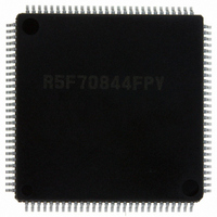
DF70844AD80FPV Renesas Electronics America, DF70844AD80FPV Datasheet - Page 1218

DF70844AD80FPV
Manufacturer Part Number
DF70844AD80FPV
Description
IC SUPERH MCU FLASH 112LQFP
Manufacturer
Renesas Electronics America
Series
SuperH® SH7080r
Datasheet
1.DF70844AD80FPV.pdf
(1644 pages)
Specifications of DF70844AD80FPV
Core Size
32-Bit
Program Memory Size
256KB (256K x 8)
Core Processor
SH-2
Speed
80MHz
Connectivity
EBI/EMI, FIFO, I²C, SCI, SSU
Peripherals
DMA, POR, PWM, WDT
Number Of I /o
76
Program Memory Type
FLASH
Ram Size
16K x 8
Voltage - Supply (vcc/vdd)
3 V ~ 5.5 V
Data Converters
A/D 8x10b
Oscillator Type
Internal
Operating Temperature
-40°C ~ 85°C
Package / Case
112-LQFP
No. Of I/o's
76
Ram Memory Size
16KB
Cpu Speed
80MHz
Digital Ic Case Style
LQFP
Supply Voltage Range
3V To 3.6V, 4.5V To 5.5V
Embedded Interface Type
I2C, SCI
Rohs Compliant
Yes
Lead Free Status / RoHS Status
Lead free / RoHS Compliant
For Use With
R0K570865S001BE - KIT STARTER FOR SH7086R0K570865S000BE - KIT STARTER FOR SH7086HS0005KCU11H - EMULATOR E10A-USB H8S(X),SH2(A)
Eeprom Size
-
Lead Free Status / RoHS Status
Lead free / RoHS Compliant, Lead free / RoHS Compliant
Available stocks
Company
Part Number
Manufacturer
Quantity
Price
Company:
Part Number:
DF70844AD80FPV
Manufacturer:
Renesas Electronics America
Quantity:
10 000
- Current page: 1218 of 1644
- Download datasheet (10Mb)
Section 21 Pin Function Controller (PFC)
21.2
1. In this LSI, the same function is available as a multiplexed function on multiple pins. This
Table 21.22 Transmit Forms of Input Functions Allocated to Multiple Pins
2. When the port input is switched from a low level to the DREQ or the IRQ edge for the pins
3. Do not set functions other than those specified in tables 21.17 to 21.20. Otherwise, correct
4. PFC setting in single-chip mode (MCU operating mode 3)
Rev. 3.00 May 17, 2007 Page 1160 of 1582
REJ09B0181-0300
OR Type
SCK0, SCK3, RXD0, RXD3,
TIOC3AS to TIOC3DS, TIOC4AS to TIOC4DS,
TIC5U, TIC5V, TIC5W, TIC5US, TIC5VS, TIC5WS
approach is intended to increase the number of selectable pin functions and to allow the easier
design of boards. If two or more pins are specified for one function, however, there are two
cautions shown below.
When the pin function is input
When the pin function is output
that are multiplexed with input/output and DREQ or IRQ, the corresponding edge is detected.
operation cannot be guaranteed.
In single-chip mode, do not set the PFC to select address bus, data bus, bus control, or the
BREQ, BACK, CK, DACK, or TEND signals. If they are selected, address bus signals
function as high- or low-level outputs, data bus signals function as high-impedance outputs,
and the other output signals function as high-level outputs. As BREQ and WAIT function as
inputs, do not leave them open. However, the bus-mastership-request inputs and external waits
are disabled.
Signals input to several pins are formed as one signal through OR or AND logic and the
signal is transmitted into the LSI. Therefore, a signal that differs from the input signals may
be transmitted to the LSI depending on the input signals in other pins that have the same
functions. Table 21.22 shows the transmit forms of input functions allocated to several
pins. When using one of the functions shown below in multiple pins, use it with care of
signal polarity considering the transmit forms.
OR type:
AND type: Signals input to several pins are formed as one signal through AND logic and
Each selected pin can output the same function.
Usage Notes
Signals input to several pins are formed as one signal through OR logic and the
signal is transmitted into the LSI.
the signal is transmitted into the LSI.
AND Type
IRQ0 to IRQ7, DREQ0, DREQ1, BREQ,
WAIT, ADTRG, POE4 to POE8
Related parts for DF70844AD80FPV
Image
Part Number
Description
Manufacturer
Datasheet
Request
R

Part Number:
Description:
KIT STARTER FOR M16C/29
Manufacturer:
Renesas Electronics America
Datasheet:

Part Number:
Description:
KIT STARTER FOR R8C/2D
Manufacturer:
Renesas Electronics America
Datasheet:

Part Number:
Description:
R0K33062P STARTER KIT
Manufacturer:
Renesas Electronics America
Datasheet:

Part Number:
Description:
KIT STARTER FOR R8C/23 E8A
Manufacturer:
Renesas Electronics America
Datasheet:

Part Number:
Description:
KIT STARTER FOR R8C/25
Manufacturer:
Renesas Electronics America
Datasheet:

Part Number:
Description:
KIT STARTER H8S2456 SHARPE DSPLY
Manufacturer:
Renesas Electronics America
Datasheet:

Part Number:
Description:
KIT STARTER FOR R8C38C
Manufacturer:
Renesas Electronics America
Datasheet:

Part Number:
Description:
KIT STARTER FOR R8C35C
Manufacturer:
Renesas Electronics America
Datasheet:

Part Number:
Description:
KIT STARTER FOR R8CL3AC+LCD APPS
Manufacturer:
Renesas Electronics America
Datasheet:

Part Number:
Description:
KIT STARTER FOR RX610
Manufacturer:
Renesas Electronics America
Datasheet:

Part Number:
Description:
KIT STARTER FOR R32C/118
Manufacturer:
Renesas Electronics America
Datasheet:

Part Number:
Description:
KIT DEV RSK-R8C/26-29
Manufacturer:
Renesas Electronics America
Datasheet:

Part Number:
Description:
KIT STARTER FOR SH7124
Manufacturer:
Renesas Electronics America
Datasheet:

Part Number:
Description:
KIT STARTER FOR H8SX/1622
Manufacturer:
Renesas Electronics America
Datasheet:

Part Number:
Description:
KIT DEV FOR SH7203
Manufacturer:
Renesas Electronics America
Datasheet:


