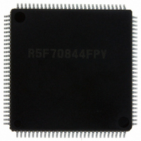
DF70844AD80FPV Renesas Electronics America, DF70844AD80FPV Datasheet - Page 33

DF70844AD80FPV
Manufacturer Part Number
DF70844AD80FPV
Description
IC SUPERH MCU FLASH 112LQFP
Manufacturer
Renesas Electronics America
Series
SuperH® SH7080r
Datasheet
1.DF70844AD80FPV.pdf
(1644 pages)
Specifications of DF70844AD80FPV
Core Size
32-Bit
Program Memory Size
256KB (256K x 8)
Core Processor
SH-2
Speed
80MHz
Connectivity
EBI/EMI, FIFO, I²C, SCI, SSU
Peripherals
DMA, POR, PWM, WDT
Number Of I /o
76
Program Memory Type
FLASH
Ram Size
16K x 8
Voltage - Supply (vcc/vdd)
3 V ~ 5.5 V
Data Converters
A/D 8x10b
Oscillator Type
Internal
Operating Temperature
-40°C ~ 85°C
Package / Case
112-LQFP
No. Of I/o's
76
Ram Memory Size
16KB
Cpu Speed
80MHz
Digital Ic Case Style
LQFP
Supply Voltage Range
3V To 3.6V, 4.5V To 5.5V
Embedded Interface Type
I2C, SCI
Rohs Compliant
Yes
Lead Free Status / RoHS Status
Lead free / RoHS Compliant
For Use With
R0K570865S001BE - KIT STARTER FOR SH7086R0K570865S000BE - KIT STARTER FOR SH7086HS0005KCU11H - EMULATOR E10A-USB H8S(X),SH2(A)
Eeprom Size
-
Lead Free Status / RoHS Status
Lead free / RoHS Compliant, Lead free / RoHS Compliant
Available stocks
Company
Part Number
Manufacturer
Quantity
Price
Company:
Part Number:
DF70844AD80FPV
Manufacturer:
Renesas Electronics America
Quantity:
10 000
- Current page: 33 of 1644
- Download datasheet (10Mb)
Figure 11.25 Example of PWM Mode Setting Procedure .......................................................... 534
Figure 11.26 Example of PWM Mode Operation (1) ................................................................. 535
Figure 11.27 Example of PWM Mode Operation (2) ................................................................. 535
Figure 11.28 Example of PWM Mode Operation (3) ................................................................. 536
Figure 11.29 Example of Phase Counting Mode Setting Procedure........................................... 537
Figure 11.30 Example of Phase Counting Mode 1 Operation .................................................... 538
Figure 11.31 Example of Phase Counting Mode 2 Operation .................................................... 539
Figure 11.32 Example of Phase Counting Mode 3 Operation .................................................... 540
Figure 11.33 Example of Phase Counting Mode 4 Operation .................................................... 541
Figure 11.34 Phase Counting Mode Application Example......................................................... 543
Figure 11.35 Procedure for Selecting Reset-Synchronized PWM Mode.................................... 545
Figure 11.36 Reset-Synchronized PWM Mode Operation Example
Figure 11.37 Block Diagram of Channels 3 and 4 in Complementary PWM Mode .................. 549
Figure 11.38 Example of Complementary PWM Mode Setting Procedure................................ 550
Figure 11.39 Complementary PWM Mode Counter Operation.................................................. 551
Figure 11.40 Example of Complementary PWM Mode Operation ............................................ 553
Figure 11.41 Example of Operation without Dead Time............................................................ 556
Figure 11.42 Example of PWM Cycle Updating........................................................................ 557
Figure 11.43 Example of Data Update in Complementary PWM Mode .................................... 559
Figure 11.44 Example of Initial Output in Complementary PWM Mode (1)............................. 560
Figure 11.45 Example of Initial Output in Complementary PWM Mode (2)............................. 561
Figure 11.46 Example of Complementary PWM Mode Waveform Output (1) ......................... 563
Figure 11.47 Example of Complementary PWM Mode Waveform Output (2) ......................... 563
Figure 11.48 Example of Complementary PWM Mode Waveform Output (3) ......................... 564
Figure 11.49 Example of Complementary PWM Mode 0% and 100% Waveform Output (1) .. 564
Figure 11.50 Example of Complementary PWM Mode 0% and 100% Waveform Output (2) .. 565
Figure 11.51 Example of Complementary PWM Mode 0% and 100% Waveform Output (3) .. 565
Figure 11.52 Example of Complementary PWM Mode 0% and 100% Waveform Output (4) .. 566
Figure 11.53 Example of Complementary PWM Mode 0% and 100% Waveform Output (5) .. 566
Figure 11.54 Example of Toggle Output Waveform Synchronized with PWM Output............. 567
Figure 11.55 Counter Clearing Synchronized with Another Channel ........................................ 568
Figure 11.56 Timing for Synchronous Counter Clearing ........................................................... 569
Figure 11.57 Example of Procedure for Setting Output Waveform Control at Synchronous
Figure 11.58 Example of Synchronous Clearing in Dead Time during Up-Counting
Figure 11.59 Example of Synchronous Clearing in Interval Tb at Crest
(When TOCR’s OLSN = 1 and OLSP = 1) ........................................................... 546
Counter Clearing in Complementary PWM Mode ................................................ 570
(Timing (3) in Figure 11.56; Bit WRE of TWCR in MTU2 is 1).......................... 571
(Timing (6) in Figure 11.56; Bit WRE of TWCR in MTU2 is 1).......................... 572
Rev. 3.00 May 17, 2007 Page xxxiii of Iviii
Related parts for DF70844AD80FPV
Image
Part Number
Description
Manufacturer
Datasheet
Request
R

Part Number:
Description:
KIT STARTER FOR M16C/29
Manufacturer:
Renesas Electronics America
Datasheet:

Part Number:
Description:
KIT STARTER FOR R8C/2D
Manufacturer:
Renesas Electronics America
Datasheet:

Part Number:
Description:
R0K33062P STARTER KIT
Manufacturer:
Renesas Electronics America
Datasheet:

Part Number:
Description:
KIT STARTER FOR R8C/23 E8A
Manufacturer:
Renesas Electronics America
Datasheet:

Part Number:
Description:
KIT STARTER FOR R8C/25
Manufacturer:
Renesas Electronics America
Datasheet:

Part Number:
Description:
KIT STARTER H8S2456 SHARPE DSPLY
Manufacturer:
Renesas Electronics America
Datasheet:

Part Number:
Description:
KIT STARTER FOR R8C38C
Manufacturer:
Renesas Electronics America
Datasheet:

Part Number:
Description:
KIT STARTER FOR R8C35C
Manufacturer:
Renesas Electronics America
Datasheet:

Part Number:
Description:
KIT STARTER FOR R8CL3AC+LCD APPS
Manufacturer:
Renesas Electronics America
Datasheet:

Part Number:
Description:
KIT STARTER FOR RX610
Manufacturer:
Renesas Electronics America
Datasheet:

Part Number:
Description:
KIT STARTER FOR R32C/118
Manufacturer:
Renesas Electronics America
Datasheet:

Part Number:
Description:
KIT DEV RSK-R8C/26-29
Manufacturer:
Renesas Electronics America
Datasheet:

Part Number:
Description:
KIT STARTER FOR SH7124
Manufacturer:
Renesas Electronics America
Datasheet:

Part Number:
Description:
KIT STARTER FOR H8SX/1622
Manufacturer:
Renesas Electronics America
Datasheet:

Part Number:
Description:
KIT DEV FOR SH7203
Manufacturer:
Renesas Electronics America
Datasheet:


