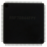
DF70844AD80FPV Renesas Electronics America, DF70844AD80FPV Datasheet - Page 1614

DF70844AD80FPV
Manufacturer Part Number
DF70844AD80FPV
Description
IC SUPERH MCU FLASH 112LQFP
Manufacturer
Renesas Electronics America
Series
SuperH® SH7080r
Datasheet
1.DF70844AD80FPV.pdf
(1644 pages)
Specifications of DF70844AD80FPV
Core Size
32-Bit
Program Memory Size
256KB (256K x 8)
Core Processor
SH-2
Speed
80MHz
Connectivity
EBI/EMI, FIFO, I²C, SCI, SSU
Peripherals
DMA, POR, PWM, WDT
Number Of I /o
76
Program Memory Type
FLASH
Ram Size
16K x 8
Voltage - Supply (vcc/vdd)
3 V ~ 5.5 V
Data Converters
A/D 8x10b
Oscillator Type
Internal
Operating Temperature
-40°C ~ 85°C
Package / Case
112-LQFP
No. Of I/o's
76
Ram Memory Size
16KB
Cpu Speed
80MHz
Digital Ic Case Style
LQFP
Supply Voltage Range
3V To 3.6V, 4.5V To 5.5V
Embedded Interface Type
I2C, SCI
Rohs Compliant
Yes
Lead Free Status / RoHS Status
Lead free / RoHS Compliant
For Use With
R0K570865S001BE - KIT STARTER FOR SH7086R0K570865S000BE - KIT STARTER FOR SH7086HS0005KCU11H - EMULATOR E10A-USB H8S(X),SH2(A)
Eeprom Size
-
Lead Free Status / RoHS Status
Lead free / RoHS Compliant, Lead free / RoHS Compliant
Available stocks
Company
Part Number
Manufacturer
Quantity
Price
Company:
Part Number:
DF70844AD80FPV
Manufacturer:
Renesas Electronics America
Quantity:
10 000
- Current page: 1614 of 1644
- Download datasheet (10Mb)
Rev. 3.00 May 17, 2007 Page 1556 of 1582
REJ09B0181-0300
Item
Figure 17.4 Example of Initial
Settings in SSU Mode
Figure 17.12 Example of Initial
Settings in Clock Synchronous
Communication Mode
18.3.1 I
(ICCR1)
2
C Bus Control Register 1
Page Revision (See Manual for Details)
882
892
906
Amended
Amended
Amended
[1]
[2]
[5]
[5]
[6]
[6]
[1]
[2]
Bit Bit Name Description
6
Specify MSS, BIDE, SOL, SCKS, CSS1,
Specify bits SDOS, SSCKOS, SCSOS,
Specify bits SDOS, SSCKOS, SCSOS,
Set PFC for external pins to be used
TENDSTS, STSATS, and SSODTS
Set PFC for external pins to be used
TENDSTS, SCSATS, and SSODTS
Specify bits TE, RE, TEIE, TIE, RIE,
Specify bits TE, RE, TEIE, TIE, RIE,
and CEIE in SSER simultaneously
Specify MSS and SCKS in SSCRH
and CEIE in SSER simultaneously
RCVD
(SSCK, SSI, SSO, and SCS)
(SSCK, SSI, SSO, and SCS)
and CSS0 bits in SSCRH
in SSCR2
in SSCR2
End
End
Reception Disable
When TRS = 0, this bit enables or disables
continuous reception without reading of ICDRR. In
master receive mode, when ICDRR cannot be read
before the rising edge of the 8th clock of SCL, set
RCVD to 1 so that data is received in byte units.
0: Enables continuous reception
1: Disables continuous reception
[1] Make appropriate settings in the PFC for the external pins to be used.
[2] Specify master/slave mode selection, bidirectional mode enable,
[3] Selects SSU mode and specify transmit/receive data length.
[4] Specify MSB first/LSB first selection, clock polarity selection,
[5] Specify open-drain output for the SSO, SSI, SSCK, and SCS pins.
[6] Enables/disables interrupt requests to the CPU.
[1] Make appropriate settings in the PFC for the external
[2] Specify master/slave mode selection and SSCK pin
[3] Selects clock synchronous communication mode and
[4] Specify clock polarity selection and transfer clock rate
[5] Specify open-drain output for the SSO, SSI, SSCK, and SCS pins.
[6] Enables/disables interrupt requests to the CPU.
SSO pin output value selection, SSCK pin selection, and SCS pin
selection.
clock phase selection, and transfer clock rate selection.
Specify timing of TEND bit setting, SCS pin assertion, and data
output on the SSO pin.
pins to be used.
selection.
specify transmit/receive data length.
selection.
Specify timing of TEND bit setting, SCS pin assertion, and data
output on the SSO pin.
Related parts for DF70844AD80FPV
Image
Part Number
Description
Manufacturer
Datasheet
Request
R

Part Number:
Description:
KIT STARTER FOR M16C/29
Manufacturer:
Renesas Electronics America
Datasheet:

Part Number:
Description:
KIT STARTER FOR R8C/2D
Manufacturer:
Renesas Electronics America
Datasheet:

Part Number:
Description:
R0K33062P STARTER KIT
Manufacturer:
Renesas Electronics America
Datasheet:

Part Number:
Description:
KIT STARTER FOR R8C/23 E8A
Manufacturer:
Renesas Electronics America
Datasheet:

Part Number:
Description:
KIT STARTER FOR R8C/25
Manufacturer:
Renesas Electronics America
Datasheet:

Part Number:
Description:
KIT STARTER H8S2456 SHARPE DSPLY
Manufacturer:
Renesas Electronics America
Datasheet:

Part Number:
Description:
KIT STARTER FOR R8C38C
Manufacturer:
Renesas Electronics America
Datasheet:

Part Number:
Description:
KIT STARTER FOR R8C35C
Manufacturer:
Renesas Electronics America
Datasheet:

Part Number:
Description:
KIT STARTER FOR R8CL3AC+LCD APPS
Manufacturer:
Renesas Electronics America
Datasheet:

Part Number:
Description:
KIT STARTER FOR RX610
Manufacturer:
Renesas Electronics America
Datasheet:

Part Number:
Description:
KIT STARTER FOR R32C/118
Manufacturer:
Renesas Electronics America
Datasheet:

Part Number:
Description:
KIT DEV RSK-R8C/26-29
Manufacturer:
Renesas Electronics America
Datasheet:

Part Number:
Description:
KIT STARTER FOR SH7124
Manufacturer:
Renesas Electronics America
Datasheet:

Part Number:
Description:
KIT STARTER FOR H8SX/1622
Manufacturer:
Renesas Electronics America
Datasheet:

Part Number:
Description:
KIT DEV FOR SH7203
Manufacturer:
Renesas Electronics America
Datasheet:


