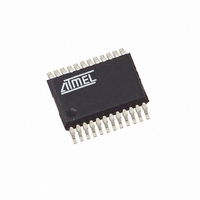
ATAM862P-TNSY4D Atmel, ATAM862P-TNSY4D Datasheet - Page 47

ATAM862P-TNSY4D
Manufacturer Part Number
ATAM862P-TNSY4D
Description
IC MCU FLASH 4K TX 433MHZ 24SSOP
Manufacturer
Atmel
Datasheet
1.ATAM862P-TNQY4D.pdf
(110 pages)
Specifications of ATAM862P-TNSY4D
Applications
UHF ASK/FSK
Core Processor
MARC4
Program Memory Type
FLASH (4 kB)
Controller Series
MARC4 4-Bit
Ram Size
256 x 4
Interface
SSI
Number Of I /o
11
Voltage - Supply
1.8 V ~ 4 V
Operating Temperature
-40°C ~ 125°C
Mounting Type
Surface Mount
Package / Case
24-SSOP
Processor Series
ATAM862x
Core
MARC4
Data Bus Width
4 bit
Mounting Style
SMD/SMT
Lead Free Status / RoHS Status
Lead free / RoHS Compliant
22.8
4551G–4BMCU–07/07
Timer 2
8-/12-bit Timer for:
Timer 2 can be used as an interval timer for interrupt generation, as signal generator or as
baud-rate generator and modulator for the serial interface. It consists of a 4-bit and an 8-bit up
counter stage which both have compare registers. The 4-bit counter stages of Timer 2 are cas-
cadable as a 12-bit timer or as an 8-bit timer with 4-bit prescaler. The timer can also be
configured as an 8-bit timer and a separate 4-bit prescaler.
The Timer 2 input can be supplied via the system clock, the external input clock (T2I), the Timer
1 output clock, the Timer 3 output clock or the shift clock of the serial interface. The external
input clock T2I is not synchronized with SYSCL. Therefore, it is possible to use Timer 2 with a
higher clock speed than SYSCL. Furthermore, with that input clock the Timer 2 operates in the
power-down mode SLEEP (CPU core -> sleep and OSC-Stop -> yes) as well as in the
POWER-DOWN (CPU core -> sleep and OSC-Stop -> no). All other clock sources supply no
clock signal in SLEEP if NSTOP = 0. The 4-bit counter stages of Timer 2 have an additional
clock output (POUT).
Its output has a modulator stage that allows the generation of pulses as well as the generation
and modulation of carrier frequencies. The Timer 2 output can modulate with the shift register
data output to generate Biphase- or Manchester code.
If the serial interface is used to modulate a bitstream, the 4-bit stage of Timer 2 has a special
task. The shift register can only handle bitstream lengths divisible by 8. For other lengths, the
4-bit counter stage can be used to stop the modulator after the right bit-count is shifted out.
If the timer is used for carrier frequency modulation, the 4-bit stage works together with an addi-
tional 2-bit duty cycle generator like a 6-bit prescaler to generate carrier frequency and duty
cycle. The 8-bit counter is used to enable and disable the modulator output for a programmable
count of pulses.
For programming the time interval, the timer has a 4-bit and an 8-bit compare register. For pro-
gramming the timer function, it has four mode and control registers. The comparator output of
stage 2 is controlled by a special compare mode register (T2CM). This register contains mask
bits for the actions (counter reset, output toggle, timer interrupt) which can be triggered by a
compare match event or the counter overflow. This architecture enables the timer function for
various modes.
The Timer 2 has a 4-bit compare register (T2CO1) and an 8-bit compare register (T2CO2). Both
these compare registers are cascadable as a 12-bit compare register, or 8-bit compare register
and 4-bit compare register.
For 12-bit compare data value:
For 8-bit compare data value:
For 4-bit compare data value:
• Interrupt, square-wave, pulse and duty cycle generation
• Baud-rate generation for the internal shift register
• Manchester and Biphase modulation together with the SSI
• Carrier frequency generation and modulation together with the SSI
m = x +1
n = y +1
l = z +1
0 ≤ x ≤ 4095
0 ≤ y ≤ 255
0 ≤ z ≤ 15
ATAM862-4
47


