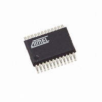
ATAM862P-TNSY4D Atmel, ATAM862P-TNSY4D Datasheet - Page 54

ATAM862P-TNSY4D
Manufacturer Part Number
ATAM862P-TNSY4D
Description
IC MCU FLASH 4K TX 433MHZ 24SSOP
Manufacturer
Atmel
Datasheet
1.ATAM862P-TNQY4D.pdf
(110 pages)
Specifications of ATAM862P-TNSY4D
Applications
UHF ASK/FSK
Core Processor
MARC4
Program Memory Type
FLASH (4 kB)
Controller Series
MARC4 4-Bit
Ram Size
256 x 4
Interface
SSI
Number Of I /o
11
Voltage - Supply
1.8 V ~ 4 V
Operating Temperature
-40°C ~ 125°C
Mounting Type
Surface Mount
Package / Case
24-SSOP
Processor Series
ATAM862x
Core
MARC4
Data Bus Width
4 bit
Mounting Style
SMD/SMT
Lead Free Status / RoHS Status
Lead free / RoHS Compliant
- Current page: 54 of 110
- Download datasheet (3Mb)
22.12.1
22.12.2
54
ATAM862-4
Timer 2 Control Register (T2C)
Timer 2 Mode Register 1 (T2M1)
Table 22-7.
Table 22-8.
T2CS1
T2CS0
T2TS
T2R
T2D1
T2D0
T2MS1
T2MS0
T2CS1
T2D1
T2CS1
T2D1
Bit 3
Bit 3
1
1
0
0
0
0
1
1
Timer 2 Clock Select bit 1
Timer 2 Clock Select bit 0
Timer 2 Toggle with Start
T2TS = 0, the output flip-flop of Timer 2 is not toggled with the timer start
T2TS = 1, the output flip-flop of Timer 2 is toggled when the timer is started with
T2R
Timer 2 Run
T2R = 0, Timer 2 stop and reset
T2R = 1, Timer 2 run
Timer 2 Mode Select bit 1
Timer 2 Mode Select bit 0
Timer 2 Duty cycle bit 1
Timer 2 Duty cycle bit 0
T2CS0
T2D0
Bit 2
Bit 2
Timer 2 Clock Select Bits
Timer 2 Duty Cycle Bits
T2D0
T2CS0
1
0
1
0
0
1
0
1
Function of Duty Cycle Generator (DCG)
Bypassed (DCGO0)
Duty cycle 1/1 (DCGO1)
Duty cycle 1/2 (DCGO2)
Duty cycle 1/3 (DCGO3)
T2MS1
T2TS
Bit 1
Bit 1
Input Clock (CL 2/1) of Counter Stage 2/1
System clock (SYSCL)
Output signal of Timer 1 (T1OUT)
Internal shift clock of SSI (SCL)
Output signal of Timer 3 (TOG3)
T2MS0
Bit 0
T2R
Bit 0
Address: "7"hex - Subaddress: "0"hex
Address: "7"hex - Subaddress: "1"hex
Reset value: 0000b
Reset value: 1111b
Additional Divider Effect
4551G–4BMCU–07/07
/1
/2
/3
/4
Related parts for ATAM862P-TNSY4D
Image
Part Number
Description
Manufacturer
Datasheet
Request
R

Part Number:
Description:
IC MCU FLASH 4K TX 315MHZ 24SSOP
Manufacturer:
Atmel
Datasheet:

Part Number:
Description:
IC MCU FLASH 4K TX 433MHZ 24SSOP
Manufacturer:
Atmel
Datasheet:

Part Number:
Description:
IC MCU FLASH 4K TX 868MHZ 24SSOP
Manufacturer:
Atmel
Datasheet:

Part Number:
Description:
IC MCU FLASH 4K TX 315MHZ 24SSOP
Manufacturer:
Atmel
Datasheet:

Part Number:
Description:
IC MCU FLASH 4K TX 868MHZ 24SSOP
Manufacturer:
Atmel
Datasheet:

Part Number:
Description:
DEV KIT FOR AVR/AVR32
Manufacturer:
Atmel
Datasheet:

Part Number:
Description:
INTERVAL AND WIPE/WASH WIPER CONTROL IC WITH DELAY
Manufacturer:
ATMEL Corporation
Datasheet:

Part Number:
Description:
Low-Voltage Voice-Switched IC for Hands-Free Operation
Manufacturer:
ATMEL Corporation
Datasheet:

Part Number:
Description:
MONOLITHIC INTEGRATED FEATUREPHONE CIRCUIT
Manufacturer:
ATMEL Corporation
Datasheet:

Part Number:
Description:
AM-FM Receiver IC U4255BM-M
Manufacturer:
ATMEL Corporation
Datasheet:

Part Number:
Description:
Monolithic Integrated Feature Phone Circuit
Manufacturer:
ATMEL Corporation
Datasheet:

Part Number:
Description:
Multistandard Video-IF and Quasi Parallel Sound Processing
Manufacturer:
ATMEL Corporation
Datasheet:


