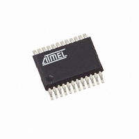
ATAM862P-TNSY4D Atmel, ATAM862P-TNSY4D Datasheet - Page 97

ATAM862P-TNSY4D
Manufacturer Part Number
ATAM862P-TNSY4D
Description
IC MCU FLASH 4K TX 433MHZ 24SSOP
Manufacturer
Atmel
Datasheet
1.ATAM862P-TNQY4D.pdf
(110 pages)
Specifications of ATAM862P-TNSY4D
Applications
UHF ASK/FSK
Core Processor
MARC4
Program Memory Type
FLASH (4 kB)
Controller Series
MARC4 4-Bit
Ram Size
256 x 4
Interface
SSI
Number Of I /o
11
Voltage - Supply
1.8 V ~ 4 V
Operating Temperature
-40°C ~ 125°C
Mounting Type
Surface Mount
Package / Case
24-SSOP
Processor Series
ATAM862x
Core
MARC4
Data Bus Width
4 bit
Mounting Style
SMD/SMT
Lead Free Status / RoHS Status
Lead free / RoHS Compliant
24.6.2
24.7
24.7.1
24.7.2
24.7.3
4551G–4BMCU–07/07
EEPROM
Control Byte Format
EEPROM – Operating Modes
Write Operations
Acknowledge Polling
The EEPROM has a size of 2 × 512 bits and is organized as 32 × 16-bit matrix each. To read
and write data to and from the EEPROM the serial interface must be used. The interface sup-
ports one and two byte write accesses and one to n-byte read accesses to the EEPROM.
The operating modes of the EEPROM are defined via the control byte. The control byte contains
the row address, the mode control bits and the read/not-write bit that is used to control the direc-
tion of the following transfer. A "0" defines a write access and a "1" a read access. The five
address bits select one of the 32 rows of the EEPROM memory to be accessed. For all
accesses the complete 16-bit word of the selected row is loaded into a buffer. The buffer must
be read or overwritten via the serial interface. The two mode control bits C1 and C2 define in
which order the accesses to the buffer are performed: High byte – low byte or low byte – high
byte. The EEPROM also supports autoincrement and autodecrement read operations. After
sending the start address with the corresponding mode, consecutive memory cells can be read
row by row without transmission of the row addresses.
Two special control bytes enable the complete initialization of EEPROM with "0" or with "1".
The EEPROM permits 8-bit and 16-bit write operations. A write access starts with the START
condition followed by a write control byte and one or two data bytes from the master. It is com-
pleted via the STOP condition from the master after the acknowledge cycle.
The programming cycle consists of an erase cycle (write "zeros") and the write cycle (write
"ones"). Both cycles together take about 10 ms.
If the EEPROM is busy with an internal write cycle, all inputs are disabled and the EEPROM will
not acknowledge until the write cycle is finished. This can be used to detect the end of the write
cycle. The master must perform acknowledge polling by sending a start condition followed by
the control byte. If the device is still busy with the write cycle, it will not return an acknowledge
and the master has to generate a stop condition or perform further acknowledge polling
sequences. If the cycle is complete, it returns an acknowledge and the master can proceed with
the next read or write cycle.
Start
Start
Control byte
A4
A3
EEPROM Address
Ackn
A2
Data byte
A1
A0
Ackn
Control Bits
C1
Mode
Data byte
C0
NWrite
Read/
R/NW
Ackn
Ackn
ATAM862-4
Stop
97


