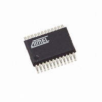
ATAM862P-TNSY4D Atmel, ATAM862P-TNSY4D Datasheet - Page 63

ATAM862P-TNSY4D
Manufacturer Part Number
ATAM862P-TNSY4D
Description
IC MCU FLASH 4K TX 433MHZ 24SSOP
Manufacturer
Atmel
Datasheet
1.ATAM862P-TNQY4D.pdf
(110 pages)
Specifications of ATAM862P-TNSY4D
Applications
UHF ASK/FSK
Core Processor
MARC4
Program Memory Type
FLASH (4 kB)
Controller Series
MARC4 4-Bit
Ram Size
256 x 4
Interface
SSI
Number Of I /o
11
Voltage - Supply
1.8 V ~ 4 V
Operating Temperature
-40°C ~ 125°C
Mounting Type
Surface Mount
Package / Case
24-SSOP
Processor Series
ATAM862x
Core
MARC4
Data Bus Width
4 bit
Mounting Style
SMD/SMT
Lead Free Status / RoHS Status
Lead free / RoHS Compliant
- Current page: 63 of 110
- Download datasheet (3Mb)
23.3
23.3.1
23.3.2
23.3.3
4551G–4BMCU–07/07
Timer 3 Modulator/Demodulator Modes
Timer 3 – Mode 6:
Carrier Frequency Burst Modulation Controlled by Timer 2 Output Toggle Flip-Flop (M2)
Timer 3 – Mode 7: Carrier Frequency Burst Modulation Controlled by SSI Internal Output (SO)
Timer 3 – Mode 8: FSK Modulation with Shift Register Data (SO)
The Timer 3 counter is driven by an internal or external clock source. Its compare- and compare
mode registers must be programmed to generate the carrier frequency via the output toggle
flip-flop. The output toggle flip-flop of Timer 2 is used to enable or disable the Timer 3 output.
Timer 2 can be driven by the toggle output signal of Timer 3 or any other clock source (see
“Combination Mode 11: Burst Modulation 1” on page
The Timer 3 counter is driven by an internal or external clock source. Its compare- and compare
mode registers must be programmed to generate the carrier frequency via the output toggle
flip-flop. The output (SO) of the SSI is used to enable or disable the Timer 3 output. The SSI
should be supplied with the toggle signal of Timer 2 (see
tion 2” on page
The two compare registers are used for generating two different time intervals. The SSI internal
data output (SO) selects which compare register is used for the output frequency generation. A
"0" level at the SSI data output enables the compare register 1. A "1" level enables compare reg-
ister 2. The compare- and compare-mode registers must be programmed to generate the two
frequencies via the output toggle flip-flop. The SSI can be supplied with the toggle signal of
Timer 2. The Timer 3 counter is driven by an internal or external clock source. The Timer 2
counter is driven by the Counter 3 (TOG3) (see
page
Figure 23-8. FSK Modulation
94).
Counter 3
CM31
CM32
T3R
T3O
SO
94).
0 1 2 3 4 0 1 2 3 4 0 1 2 3
0
4 0 1 2 0 1 2 0 1 2 0 1 2 0 1 2 0 1 2 0 1 2 0 1 2 3
“Combination Mode 13: FSK Modulation” on
92).
1
“Combination Mode 12: Burst Modula-
ATAM862-4
0
4 0
1
63
Related parts for ATAM862P-TNSY4D
Image
Part Number
Description
Manufacturer
Datasheet
Request
R

Part Number:
Description:
IC MCU FLASH 4K TX 315MHZ 24SSOP
Manufacturer:
Atmel
Datasheet:

Part Number:
Description:
IC MCU FLASH 4K TX 433MHZ 24SSOP
Manufacturer:
Atmel
Datasheet:

Part Number:
Description:
IC MCU FLASH 4K TX 868MHZ 24SSOP
Manufacturer:
Atmel
Datasheet:

Part Number:
Description:
IC MCU FLASH 4K TX 315MHZ 24SSOP
Manufacturer:
Atmel
Datasheet:

Part Number:
Description:
IC MCU FLASH 4K TX 868MHZ 24SSOP
Manufacturer:
Atmel
Datasheet:

Part Number:
Description:
DEV KIT FOR AVR/AVR32
Manufacturer:
Atmel
Datasheet:

Part Number:
Description:
INTERVAL AND WIPE/WASH WIPER CONTROL IC WITH DELAY
Manufacturer:
ATMEL Corporation
Datasheet:

Part Number:
Description:
Low-Voltage Voice-Switched IC for Hands-Free Operation
Manufacturer:
ATMEL Corporation
Datasheet:

Part Number:
Description:
MONOLITHIC INTEGRATED FEATUREPHONE CIRCUIT
Manufacturer:
ATMEL Corporation
Datasheet:

Part Number:
Description:
AM-FM Receiver IC U4255BM-M
Manufacturer:
ATMEL Corporation
Datasheet:

Part Number:
Description:
Monolithic Integrated Feature Phone Circuit
Manufacturer:
ATMEL Corporation
Datasheet:

Part Number:
Description:
Multistandard Video-IF and Quasi Parallel Sound Processing
Manufacturer:
ATMEL Corporation
Datasheet:


