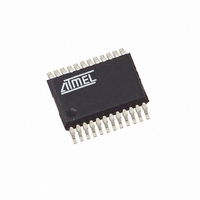
ATAM862P-TNSY4D Atmel, ATAM862P-TNSY4D Datasheet - Page 72

ATAM862P-TNSY4D
Manufacturer Part Number
ATAM862P-TNSY4D
Description
IC MCU FLASH 4K TX 433MHZ 24SSOP
Manufacturer
Atmel
Datasheet
1.ATAM862P-TNQY4D.pdf
(110 pages)
Specifications of ATAM862P-TNSY4D
Applications
UHF ASK/FSK
Core Processor
MARC4
Program Memory Type
FLASH (4 kB)
Controller Series
MARC4 4-Bit
Ram Size
256 x 4
Interface
SSI
Number Of I /o
11
Voltage - Supply
1.8 V ~ 4 V
Operating Temperature
-40°C ~ 125°C
Mounting Type
Surface Mount
Package / Case
24-SSOP
Processor Series
ATAM862x
Core
MARC4
Data Bus Width
4 bit
Mounting Style
SMD/SMT
Lead Free Status / RoHS Status
Lead free / RoHS Compliant
23.8
23.8.1
23.8.2
72
Synchronous Serial Interface (SSI)
ATAM862-4
SSI Features:
SSI Peripheral Configuration
The synchronous serial interface (SSI) can be used either for serial communication with external
devices such as EEPROMs, shift registers, display drivers, other microcontrollers, or as a
means for generating and capturing on-chip serial streams of data. External data communication
takes place via the Port 4 (BP4),a multi-functional port which can be software configured by writ-
ing the appropriate control word into the P4CR register. The SSI can be configured in any of the
following ways:
• With Timer 1
• With Timer 2
• With Timer 3
1. 2-wire external interface for bi-directional data communication with one data terminal
2. 3-wire external interface for simultaneous input and output of serial data, with a serial
3. Timer/SSI combined modes – the SSI used together with Timer 2 or Timer 3 is capable
– 2- and 3-wire NRZ
– 2-wire mode multi-chip link mode (MCL), additional internal 2-wire link for multi-chip
– Biphase modulation
– Manchester modulation
– Pulse-width demodulation
– Burst modulation
– Pulse-width modulation (PWM)
– FSK modulation
– Biphase demodulation
– Manchester demodulation
– Pulse-width demodulation
– Pulse position Demodulation
and one shift clock. The SSI uses the Port BP43 as a bi-directional serial data line (SD)
and BP40 as shift clock line (SC).
input data terminal (SI), a serial output data terminal (SO) and a shift clock (SC). The
SSI uses BP40 as shift clock (SC), while the serial data input (SI) is applied to BP43
(configured in P4CR as input). Serial output data (SO) in this case is passed through to
BP42 (configured in P4CR to T2O) via the Timer 2 output stage (T2M2 configured in
mode 6).
of performing a variety of data modulation and demodulation functions (see section
Timer). The modulating data is converted by the SSI into a continuous serial stream of
data which is in turn modulated in one of the timer functional blocks. Serial demodu-
lated data can be serially captured in the SSI and read by the controller. In the Timer 3
modes 10 and 11 (demodulation modes) the SSI can only be used as demodulator.
packaging solutions
4551G–4BMCU–07/07


