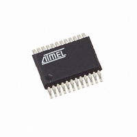
ATAM862P-TNSY4D Atmel, ATAM862P-TNSY4D Datasheet - Page 78

ATAM862P-TNSY4D
Manufacturer Part Number
ATAM862P-TNSY4D
Description
IC MCU FLASH 4K TX 433MHZ 24SSOP
Manufacturer
Atmel
Datasheet
1.ATAM862P-TNQY4D.pdf
(110 pages)
Specifications of ATAM862P-TNSY4D
Applications
UHF ASK/FSK
Core Processor
MARC4
Program Memory Type
FLASH (4 kB)
Controller Series
MARC4 4-Bit
Ram Size
256 x 4
Interface
SSI
Number Of I /o
11
Voltage - Supply
1.8 V ~ 4 V
Operating Temperature
-40°C ~ 125°C
Mounting Type
Surface Mount
Package / Case
24-SSOP
Processor Series
ATAM862x
Core
MARC4
Data Bus Width
4 bit
Mounting Style
SMD/SMT
Lead Free Status / RoHS Status
Lead free / RoHS Compliant
- Current page: 78 of 110
- Download datasheet (3Mb)
23.8.8
78
ATAM862-4
SSI Interrupt
Figure 23-21. MCL Bus Protocol 1
Bus not busy (1)
Start data transfer (2)
Stop data transfer (3)
Data valid (4)
Acknowledge
Figure 23-22. MCL Bus Protocol 2
The SSI interrupt INT3 can be generated either by an SSI buffer register status (i.e., transmit
buffer empty or receive buffer full), the end of SSI data telegram or on the falling edge of the
SC/SD pins on Port 4 (see
rupt selection is performed by the Interrupt FunctioN control bit (IFN). The SSI interrupt is usually
used to synchronize the software control of the SSI and inform the controller of the present SSI
status. The Port 4 interrupts can be used together with the SSI or, if the SSI itself is not required,
as additional external interrupt sources. In either case this interrupt is capable of waking the con-
troller out of sleep mode.
To enable and select the SSI relevant interrupts use the SSI interrupt mask (SIM) and the Inter-
rupt Function (IFN) while the Port 4 interrupts are enabled by setting appropriate control bits in
P4CR register.
SC
SD
SC
SD
(1)
Start
condition
Start
(2)
1st Bit
1
“Port 4 Control Register (P4CR) Byte Write” on page
Both data and clock lines remain HIGH.
A HIGH to LOW transition of the SD line while the clock (SC)
is HIGH defines a START condition.
A LOW to HIGH transition of the SD line while the clock (SC)
is HIGH defines a STOP condition.
The state of the data line represents valid data when,
after START condition, the data line is stable for the
duration of the HIGH period of the clock signal.
All address and data words are serially transmitted to and
from the device in eight-bit words. The receiving device
returns a zero on the data line during the ninth clock cycle to
acknowledge word receipt.
Data
valid
(4)
n
change
Data
8th Bit
8
valid
Data
(4)
ACK
9
condition
4551G–4BMCU–07/07
Stop
40). SSI inter-
Stop
(3)
(1)
Related parts for ATAM862P-TNSY4D
Image
Part Number
Description
Manufacturer
Datasheet
Request
R

Part Number:
Description:
IC MCU FLASH 4K TX 315MHZ 24SSOP
Manufacturer:
Atmel
Datasheet:

Part Number:
Description:
IC MCU FLASH 4K TX 433MHZ 24SSOP
Manufacturer:
Atmel
Datasheet:

Part Number:
Description:
IC MCU FLASH 4K TX 868MHZ 24SSOP
Manufacturer:
Atmel
Datasheet:

Part Number:
Description:
IC MCU FLASH 4K TX 315MHZ 24SSOP
Manufacturer:
Atmel
Datasheet:

Part Number:
Description:
IC MCU FLASH 4K TX 868MHZ 24SSOP
Manufacturer:
Atmel
Datasheet:

Part Number:
Description:
DEV KIT FOR AVR/AVR32
Manufacturer:
Atmel
Datasheet:

Part Number:
Description:
INTERVAL AND WIPE/WASH WIPER CONTROL IC WITH DELAY
Manufacturer:
ATMEL Corporation
Datasheet:

Part Number:
Description:
Low-Voltage Voice-Switched IC for Hands-Free Operation
Manufacturer:
ATMEL Corporation
Datasheet:

Part Number:
Description:
MONOLITHIC INTEGRATED FEATUREPHONE CIRCUIT
Manufacturer:
ATMEL Corporation
Datasheet:

Part Number:
Description:
AM-FM Receiver IC U4255BM-M
Manufacturer:
ATMEL Corporation
Datasheet:

Part Number:
Description:
Monolithic Integrated Feature Phone Circuit
Manufacturer:
ATMEL Corporation
Datasheet:

Part Number:
Description:
Multistandard Video-IF and Quasi Parallel Sound Processing
Manufacturer:
ATMEL Corporation
Datasheet:


