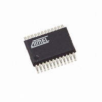
ATAM862P-TNSY4D Atmel, ATAM862P-TNSY4D Datasheet - Page 74

ATAM862P-TNSY4D
Manufacturer Part Number
ATAM862P-TNSY4D
Description
IC MCU FLASH 4K TX 433MHZ 24SSOP
Manufacturer
Atmel
Datasheet
1.ATAM862P-TNQY4D.pdf
(110 pages)
Specifications of ATAM862P-TNSY4D
Applications
UHF ASK/FSK
Core Processor
MARC4
Program Memory Type
FLASH (4 kB)
Controller Series
MARC4 4-Bit
Ram Size
256 x 4
Interface
SSI
Number Of I /o
11
Voltage - Supply
1.8 V ~ 4 V
Operating Temperature
-40°C ~ 125°C
Mounting Type
Surface Mount
Package / Case
24-SSOP
Processor Series
ATAM862x
Core
MARC4
Data Bus Width
4 bit
Mounting Style
SMD/SMT
Lead Free Status / RoHS Status
Lead free / RoHS Compliant
23.8.4
74
ATAM862-4
8-bit Synchronous Mode
At the beginning of every telegram, the SSI control loads the transmit buffer into the shift register
and proceeds immediately to shift data serially out. At the same time, incoming data is shifted
into the shift register input. This incoming data is automatically loaded into the receive buffer
when the complete telegram has been received. Thus, data can be simultaneously received and
transmitted if required.
Before data can be transferred, the SSI must first be activated. This is performed by means of
the SSI reset control (SIR) bit. All further operation then depends on the data directional mode
(TX/RX) and the present status of the SSI buffer registers shown by the Serial Interface Ready
Status Flag (SRDY). This SRDY flag indicates the (empty/full) status of either the transmit buffer
(in TX mode), or the receive buffer (in RX mode). The control logic ensures that data shifting is
temporarily halted at any time, if the appropriate receive/transmit buffer is not ready (SRDY = 0).
The SRDY status will then automatically be set back to ‘1’ and data shifting resumed as soon as
the application software loads the new data into the transmit register (in TX mode) or frees the
shift register by reading it into the receive buffer (in RX mode).
A further activity status (ACT) bit indicates the present status of the serial communication. The
ACT bit remains high for the duration of the serial telegram or if MCL stop or start conditions are
currently being generated. Both the current SRDY and ACT status can be read in the SSI status
register. To deactivate the SSI, the SIR bit must be set high.
Figure 23-16. 8-bit Synchronous Mode
In the 8-bit synchronous mode, the SSI can operate as either a 2- or 3-wire interface (see
Peripheral Configuration” on page
format, synchronized to either the rising or falling edge of the shift clock (SC). The choice of
clock edge is defined by the Serial Mode Control bits (SM0,SM1). It should be noted that the
transmission edge refers to the SC clock edge with which the SD changes. To avoid clock skew
problems, the incoming serial input data is shifted in with the opposite edge.
When used together with one of the timer modulator or demodulator stages, the SSI must be set
in the 8-bit synchronous mode 1.
In RX mode, as soon as the SSI is activated (SIR = 0), 8 shift clocks are generated and the
incoming serial data is shifted into the shift register. This first telegram is automatically trans-
ferred into the receive buffer and the SRDY set to 0 indicating that the receive buffer contains
valid data. At the same time an interrupt (if enabled) is generated. The SSI then continues shift-
ing in the following 8-bit telegram. If, during this time the first telegram has been read by the
controller, the second telegram will also be transferred in the same way into the receive buffer
(Falling edge)
(Rising edge)
SD/TO2
DATA
SC
SC
Data: 00110101
Bit 7
Bit 7
0
0
0
0
72). The serial data (SD) is received or transmitted in NRZ
1
1
1
1
0
0
1
1
0
0
Bit 0
Bit 0
1
1
4551G–4BMCU–07/07
“SSI


