ATAM862P-TNSY4D Atmel, ATAM862P-TNSY4D Datasheet - Page 73

ATAM862P-TNSY4D
Manufacturer Part Number
ATAM862P-TNSY4D
Description
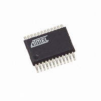
IC MCU FLASH 4K TX 433MHZ 24SSOP
Manufacturer
Atmel
Datasheet
1.ATAM862P-TNQY4D.pdf
(110 pages)
Specifications of ATAM862P-TNSY4D
Applications
UHF ASK/FSK
Core Processor
MARC4
Program Memory Type
FLASH (4 kB)
Controller Series
MARC4 4-Bit
Ram Size
256 x 4
Interface
SSI
Number Of I /o
11
Voltage - Supply
1.8 V ~ 4 V
Operating Temperature
-40°C ~ 125°C
Mounting Type
Surface Mount
Package / Case
24-SSOP
Processor Series
ATAM862x
Core
MARC4
Data Bus Width
4 bit
Mounting Style
SMD/SMT
Lead Free Status / RoHS Status
Lead free / RoHS Compliant
23.8.3
4551G–4BMCU–07/07
General SSI Operation
Figure 23-15. Block Diagram of the Synchronous Serial Interface
The SSI is comprised essentially of an 8-bit shift register with two associated 8-bit buffers – the
receive buffer (SRB) for capturing the incoming serial data and a transmit buffer (STB) for inter-
mediate storage of data to be serially output. Both buffers are directly accessable by software.
Transferring the parallel buffer data into and out of the shift register is controlled automatically by
the SSI control, so that both single byte transfers or continuous bit streams can be supported.
The SSI can generate the shift clock (SC) either from one of several on-chip clock sources or
accept an external clock. The external shift clock is output on, or applied to the Port BP40.
Selection of an external clock source is performed by the Serial Clock Direction control bit
(SCD). In the combinational modes, the required clock is selected by the corresponding timer
mode.
The SSI can operate in three data transfer modes – synchronous 8-bit shift mode, a 9-bit
Multi-Chip Link Mode (MCL) ,or 8-bit pseudo MCL protocol (without acknowledge-bit).
External SSI clocking is not supported in these modes. The SSI should thus generate and has
full control over the shift clock so that it can always be regarded as an MCL bus master device.
All directional control of the external data port used by the SSI is handled automatically and is
dependent on the transmission direction set by the Serial Data Direction (SDD) control bit. This
control bit defines whether the SSI is currently operating in Transmit (TX) mode or Receive (RX)
mode.
Serial data is organized in 8-bit telegrams which are shifted with the most significant bit first. In
the 9-bit MCL mode, an additional acknowledge bit is appended to the end of the telegram for
handshaking purposes (see
4. Multi-chip link (MCL) – the SSI can also be used as an interchip data interface for use in
T1OUT
SYSCL
TOG2
POUT
single package multi-chip modules or hybrids. For such applications, the SSI is pro-
vided with two dedicated pads (MCL_SD and MCL_SC) which act as a two-wire
chip-to-chip link. The MCL can be activated by the MCL control bit. Should these MCL
pads be used by the SSI, the standard SD and SC pins are not required and the corre-
sponding Port 4 ports are available as conventional data ports.
SIC1
/2
SC
“MCL Bus Protocol” on page
Shift_CL
SO
Transmit
Buffer
I/O-bus
SIC2
MSB
STB
SSI-Control
8-bit Shift Register
I/O-bus
SISC
SRB
Control
77).
LSB
Receive
Buffer
Timer 2 / Timer 3
SI
INT3
SO
Output
ATAM862-4
SI
SCI
SC
MCL_SC
MCL_SD
SD
73


