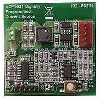
MCP1631RD-MCC1 Microchip Technology, MCP1631RD-MCC1 Datasheet - Page 105

MCP1631RD-MCC1
Manufacturer Part Number
MCP1631RD-MCC1
Description
REFERENCE DESIGN FOR MCP1631HV
Manufacturer
Microchip Technology
Type
Battery Managementr
Datasheets
1.MCP1631VHVT-330EST.pdf
(34 pages)
2.MCP1631HV-330EST.pdf
(54 pages)
3.MCP1631RD-MCC2.pdf
(20 pages)
4.MCP1631RD-MCC2.pdf
(328 pages)
5.MCP1631RD-MCC1.pdf
(28 pages)
Specifications of MCP1631RD-MCC1
Main Purpose
Power Management, Battery Charger
Embedded
Yes, MCU, 8-Bit
Utilized Ic / Part
MCP1631HV, PIC16F883
Primary Attributes
1 ~ 2 Cell- Li-Ion, 1 ~ 4 Cell- NiCd/NiMH
Secondary Attributes
Status LEDs
Supported Devices
MCP1631HV, PIC16F883 Device Type
Tool / Board Applications
Power Management-Battery Management
Development Tool Type
Reference Design
Input Voltage
5.5 V to 16 V
Product
Power Management Modules
Mcu Supported Families
MCP1631HV/PIC16F883 Family
Silicon Manufacturer
Microchip
Silicon Core Number
MCP1631HV
Kit Application Type
Reference Design
Application Sub Type
Battery Charger
Kit Contents
Board Only
Lead Free Status / RoHS Status
Lead free / RoHS Compliant
For Use With/related Products
MCP1631HV, PIC16F883
Lead Free Status / RoHS Status
Lead free / RoHS Compliant
- MCP1631VHVT-330EST PDF datasheet
- MCP1631HV-330EST PDF datasheet #2
- MCP1631RD-MCC2 PDF datasheet #3
- MCP1631RD-MCC2 PDF datasheet #4
- MCP1631RD-MCC1 PDF datasheet #5
- Current page: 105 of 328
- Download datasheet (6Mb)
9.2.6
This is an example procedure for using the ADC to
perform an Analog-to-Digital conversion:
1.
2.
3.
4.
5.
6.
7.
8.
© 2009 Microchip Technology Inc.
Note 1: The global interrupt can be disabled if the
Configure Port:
• Disable pin output driver (See TRIS register)
• Configure pin as analog
Configure the ADC module:
• Select ADC conversion clock
• Configure voltage reference
• Select ADC input channel
• Select result format
• Turn on ADC module
Configure ADC interrupt (optional):
• Clear ADC interrupt flag
• Enable ADC interrupt
• Enable peripheral interrupt
• Enable global interrupt
Wait the required acquisition time
Start conversion by setting the GO/DONE bit.
Wait for ADC conversion to complete by one of
the following:
• Polling the GO/DONE bit
• Waiting for the ADC interrupt (interrupts
Read ADC Result
Clear the ADC interrupt flag (required if interrupt
is enabled).
enabled)
2: See
A/D CONVERSION PROCEDURE
user is attempting to wake-up from Sleep
and resume in-line code execution.
Requirements”.
Section 9.3
(1)
“A/D
(2)
.
Acquisition
PIC16F882/883/884/886/887
EXAMPLE 9-1:
;This code block configures the ADC
;for polling, Vdd and Vss as reference, Frc
clock and AN0 input.
;
;Conversion start & polling for completion
; are included.
;
BANKSEL
MOVLW
MOVWF
BANKSEL
BSF
BANKSEL
BSF
BANKSEL
MOVLW
MOVWF
CALL
BSF
BTFSC
GOTO
BANKSEL
MOVF
MOVWF
BANKSEL
MOVF
MOVWF
ADCON1
B’10000000’ ;right justify
ADCON1
TRISA
TRISA,0
ANSEL
ANSEL,0
ADCON0
B’11000001’ ;ADC Frc clock,
ADCON0
SampleTime
ADCON0,GO
ADCON0,GO
$-1
ADRESH
ADRESH,W
RESULTHI
ADRESL
ADRESL,W
RESULTLO
A/D CONVERSION
;
;Vdd and Vss as Vref
;
;Set RA0 to input
;
;Set RA0 to analog
;
;AN0, On
;Acquisiton delay
;Start conversion
;Is conversion done?
;No, test again
;
;Read upper 2 bits
;store in GPR space
;
;Read lower 8 bits
;Store in GPR space
DS41291F-page 103
Related parts for MCP1631RD-MCC1
Image
Part Number
Description
Manufacturer
Datasheet
Request
R

Part Number:
Description:
REFERENCE DESIGN MCP1631HV
Manufacturer:
Microchip Technology
Datasheet:

Part Number:
Description:
REF DES BATT CHARG OR LED DRIVER
Manufacturer:
Microchip Technology
Datasheet:

Part Number:
Description:
Manufacturer:
Microchip Technology Inc.
Datasheet:

Part Number:
Description:
Manufacturer:
Microchip Technology Inc.
Datasheet:

Part Number:
Description:
Manufacturer:
Microchip Technology Inc.
Datasheet:

Part Number:
Description:
Manufacturer:
Microchip Technology Inc.
Datasheet:

Part Number:
Description:
Manufacturer:
Microchip Technology Inc.
Datasheet:

Part Number:
Description:
Manufacturer:
Microchip Technology Inc.
Datasheet:

Part Number:
Description:
Manufacturer:
Microchip Technology Inc.
Datasheet:

Part Number:
Description:
Manufacturer:
Microchip Technology Inc.
Datasheet:


