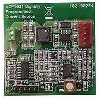
MCP1631RD-MCC1 Microchip Technology, MCP1631RD-MCC1 Datasheet - Page 273

MCP1631RD-MCC1
Manufacturer Part Number
MCP1631RD-MCC1
Description
REFERENCE DESIGN FOR MCP1631HV
Manufacturer
Microchip Technology
Type
Battery Managementr
Datasheets
1.MCP1631VHVT-330EST.pdf
(34 pages)
2.MCP1631HV-330EST.pdf
(54 pages)
3.MCP1631RD-MCC2.pdf
(20 pages)
4.MCP1631RD-MCC2.pdf
(328 pages)
5.MCP1631RD-MCC1.pdf
(28 pages)
Specifications of MCP1631RD-MCC1
Main Purpose
Power Management, Battery Charger
Embedded
Yes, MCU, 8-Bit
Utilized Ic / Part
MCP1631HV, PIC16F883
Primary Attributes
1 ~ 2 Cell- Li-Ion, 1 ~ 4 Cell- NiCd/NiMH
Secondary Attributes
Status LEDs
Supported Devices
MCP1631HV, PIC16F883 Device Type
Tool / Board Applications
Power Management-Battery Management
Development Tool Type
Reference Design
Input Voltage
5.5 V to 16 V
Product
Power Management Modules
Mcu Supported Families
MCP1631HV/PIC16F883 Family
Silicon Manufacturer
Microchip
Silicon Core Number
MCP1631HV
Kit Application Type
Reference Design
Application Sub Type
Battery Charger
Kit Contents
Board Only
Lead Free Status / RoHS Status
Lead free / RoHS Compliant
For Use With/related Products
MCP1631HV, PIC16F883
Lead Free Status / RoHS Status
Lead free / RoHS Compliant
- MCP1631VHVT-330EST PDF datasheet
- MCP1631HV-330EST PDF datasheet #2
- MCP1631RD-MCC2 PDF datasheet #3
- MCP1631RD-MCC2 PDF datasheet #4
- MCP1631RD-MCC1 PDF datasheet #5
- Current page: 273 of 328
- Download datasheet (6Mb)
TABLE 17-16: I
© 2009 Microchip Technology Inc.
Note 1:
Param.
100*
101*
102*
103*
106*
107*
109*
110*
No.
90*
91*
92*
2:
*
These parameters are characterized but not tested.
As a transmitter, the device must provide this internal minimum delay time to bridge the undefined region
(min. 300 ns) of the falling edge of SCL to avoid unintended generation of Start or Stop conditions.
A Fast mode (400 kHz) I
requirement T
stretch the low period of the SCL signal. If such a device does stretch the low period of the SCL signal, it
must output the next data bit to the SDA line T
Standard mode I
T
T
T
T
T
T
T
T
T
T
T
C
Symbol
SU
SU
SU
AA
HIGH
LOW
R
F
HD
HD
BUF
B
:
:
:
:
:
STA
DAT
STO
STA
DAT
2
C™ BUS DATA REQUIREMENTS
Clock high time
Clock low time
SDA and SCL rise
time
SDA and SCL fall
time
Start condition
setup time
Start condition hold
time
Data input hold time 100 kHz mode
Data input setup
time
Stop condition
setup time
Output valid from
clock
Bus free time
Bus capacitive loading
SU
:
2
DAT
C bus specification), before the SCL line is released.
≥ 250 ns must then be met. This will automatically be the case if the device does not
Characteristic
2
C bus device can be used in a Standard mode (100 kHz) I
100 kHz mode
400 kHz mode
SSP Module
100 kHz mode
400 kHz mode
SSP Module
100 kHz mode
400 kHz mode
100 kHz mode
400 kHz mode
100 kHz mode
400 kHz mode
100 kHz mode
400 kHz mode
400 kHz mode
100 kHz mode
400 kHz mode
100 kHz mode
400 kHz mode
100 kHz mode
400 kHz mode
100 kHz mode
400 kHz mode
PIC16F882/883/884/886/887
R
max. + T
20 + 0.1C
20 + 0.1C
1.5T
1.5T
Min.
250
100
4.0
0.6
4.7
1.3
4.7
0.6
4.0
0.6
4.7
0.6
4.7
1.3
—
—
—
—
—
0
0
SU
CY
CY
:
DAT
B
B
Max.
1000
3500
= 1000 + 250 = 1250 ns (according to the
300
300
300
0.9
400
—
—
—
—
—
—
—
—
—
—
—
—
—
—
—
—
—
—
Units
μs
μs
μs
μs
ns
ns
ns
ns
μs
μs
μs
μs
ns
μs
ns
ns
μs
μs
ns
ns
μs
μs
pF
Device must operate at a
minimum of 1.5 MHz
Device must operate at a
minimum of 10 MHz
Device must operate at a
minimum of 1.5 MHz
Device must operate at a
minimum of 10 MHz
C
10-400 pF
C
10-400 pF
Only relevant for
Repeated Start condition
After this period the first
clock pulse is generated
(Note 2)
(Note 1)
Time the bus must be free
before a new transmission
can start
B
B
2
is specified to be from
is specified to be from
C bus system, but the
Conditions
DS41291F-page 271
Related parts for MCP1631RD-MCC1
Image
Part Number
Description
Manufacturer
Datasheet
Request
R

Part Number:
Description:
REFERENCE DESIGN MCP1631HV
Manufacturer:
Microchip Technology
Datasheet:

Part Number:
Description:
REF DES BATT CHARG OR LED DRIVER
Manufacturer:
Microchip Technology
Datasheet:

Part Number:
Description:
Manufacturer:
Microchip Technology Inc.
Datasheet:

Part Number:
Description:
Manufacturer:
Microchip Technology Inc.
Datasheet:

Part Number:
Description:
Manufacturer:
Microchip Technology Inc.
Datasheet:

Part Number:
Description:
Manufacturer:
Microchip Technology Inc.
Datasheet:

Part Number:
Description:
Manufacturer:
Microchip Technology Inc.
Datasheet:

Part Number:
Description:
Manufacturer:
Microchip Technology Inc.
Datasheet:

Part Number:
Description:
Manufacturer:
Microchip Technology Inc.
Datasheet:

Part Number:
Description:
Manufacturer:
Microchip Technology Inc.
Datasheet:


