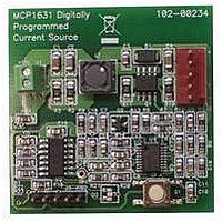
MCP1631RD-MCC1 Microchip Technology, MCP1631RD-MCC1 Datasheet - Page 254

MCP1631RD-MCC1
Manufacturer Part Number
MCP1631RD-MCC1
Description
REFERENCE DESIGN FOR MCP1631HV
Manufacturer
Microchip Technology
Type
Battery Managementr
Datasheets
1.MCP1631VHVT-330EST.pdf
(34 pages)
2.MCP1631HV-330EST.pdf
(54 pages)
3.MCP1631RD-MCC2.pdf
(20 pages)
4.MCP1631RD-MCC2.pdf
(328 pages)
5.MCP1631RD-MCC1.pdf
(28 pages)
Specifications of MCP1631RD-MCC1
Main Purpose
Power Management, Battery Charger
Embedded
Yes, MCU, 8-Bit
Utilized Ic / Part
MCP1631HV, PIC16F883
Primary Attributes
1 ~ 2 Cell- Li-Ion, 1 ~ 4 Cell- NiCd/NiMH
Secondary Attributes
Status LEDs
Supported Devices
MCP1631HV, PIC16F883 Device Type
Tool / Board Applications
Power Management-Battery Management
Development Tool Type
Reference Design
Input Voltage
5.5 V to 16 V
Product
Power Management Modules
Mcu Supported Families
MCP1631HV/PIC16F883 Family
Silicon Manufacturer
Microchip
Silicon Core Number
MCP1631HV
Kit Application Type
Reference Design
Application Sub Type
Battery Charger
Kit Contents
Board Only
Lead Free Status / RoHS Status
Lead free / RoHS Compliant
For Use With/related Products
MCP1631HV, PIC16F883
Lead Free Status / RoHS Status
Lead free / RoHS Compliant
- MCP1631VHVT-330EST PDF datasheet
- MCP1631HV-330EST PDF datasheet #2
- MCP1631RD-MCC2 PDF datasheet #3
- MCP1631RD-MCC2 PDF datasheet #4
- MCP1631RD-MCC1 PDF datasheet #5
- Current page: 254 of 328
- Download datasheet (6Mb)
PIC16F882/883/884/886/887
17.5
DS41291F-page 252
DC CHARACTERISTICS
D100
D101*
D101A* C
D120
D120A
D121
D122
D123
D124
D130
D130A
D131
D132
D133
D134
Note 1:
Param
No.
2:
3:
4:
5:
*
†
I
COSC2
E
E
V
T
T
T
E
E
V
V
T
T
DC Characteristics:
ULP
DEW
RETD
REF
PEW
RETD
D
D
DRW
P
D
PR
PEW
Sym.
IO
These parameters are characterized but not tested.
Data in “Typ” column is at 5.0V, 25°C unless otherwise stated. These parameters are for design guidance only and are
not tested.
In RC oscillator configuration, the OSC1/CLKIN pin is a Schmitt Trigger input. It is not recommended to use an external
clock in RC mode.
Negative current is defined as current sourced by the pin.
The leakage current on the MCLR pin is strongly dependent on the applied voltage level. The specified levels represent
normal operating conditions. Higher leakage current may be measured at different input voltages.
See Section 10.3.1 “Using the Data EEPROM” for additional information.
Including OSC2 in CLKOUT mode.
Ultra Low-Power Wake-Up
Current
Capacitive Loading Specs on
Output Pins
OSC2 pin
All I/O pins
Data EEPROM Memory
Byte Endurance
Byte Endurance
V
Erase/Write Cycle Time
Characteristic Retention
Number of Total Erase/Write
Cycles before Refresh
Program Flash Memory
Cell Endurance
Cell Endurance
V
V
V
Erase/Write cycle time
Characteristic Retention
DD
DD
DD
DD
for Read/Write
for Read
for Row Erase/Write
for Bulk Erase Operations
Characteristic
(4)
PIC16F883/884/886/887-I (Industrial)
PIC16F883/884/886/887-E (Extended) (Continued)
Standard Operating Conditions (unless otherwise stated)
Operating temperature
100K
Min.
V
V
V
10K
10K
1M
4.5
40
1K
40
—
—
—
—
—
MIN
MIN
MIN
Typ†
100K
100K
10M
10K
200
1M
—
—
—
—
—
—
—
—
5
2
Max.
5.5
5.5
5.5
5.5
2.5
15
50
—
—
—
—
—
—
—
—
-40°C ≤ T
-40°C ≤ T
6
Units
Year Provided no other specifications
Year Provided no other specifications
E/W -40°C ≤ T
E/W +85°C ≤ T
E/W -40°C ≤ T
E/W -40°C ≤ T
E/W +85°C ≤ T
nA
ms
ms
pF
pF
V
V
V
V
A
A
≤ +85°C for industrial
≤ +125°C for extended
© 2009 Microchip Technology Inc.
See Application Note AN879,
“Using the Microchip Ultra
Low-Power Wake-up Module”
(DS00879)
In XT, HS and LP modes when
external clock is used to drive
OSC1
Using EECON1 to read/write
V
voltage
are violated
V
voltage
are violated
MIN
MIN
= Minimum operating
= Minimum operating
A
A
A
Conditions
A
A
≤ +85°C
≤ +85°C
≤ +85°C
≤ +125°C
≤ +125°C
Related parts for MCP1631RD-MCC1
Image
Part Number
Description
Manufacturer
Datasheet
Request
R

Part Number:
Description:
REFERENCE DESIGN MCP1631HV
Manufacturer:
Microchip Technology
Datasheet:

Part Number:
Description:
REF DES BATT CHARG OR LED DRIVER
Manufacturer:
Microchip Technology
Datasheet:

Part Number:
Description:
Manufacturer:
Microchip Technology Inc.
Datasheet:

Part Number:
Description:
Manufacturer:
Microchip Technology Inc.
Datasheet:

Part Number:
Description:
Manufacturer:
Microchip Technology Inc.
Datasheet:

Part Number:
Description:
Manufacturer:
Microchip Technology Inc.
Datasheet:

Part Number:
Description:
Manufacturer:
Microchip Technology Inc.
Datasheet:

Part Number:
Description:
Manufacturer:
Microchip Technology Inc.
Datasheet:

Part Number:
Description:
Manufacturer:
Microchip Technology Inc.
Datasheet:

Part Number:
Description:
Manufacturer:
Microchip Technology Inc.
Datasheet:


