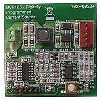
MCP1631RD-MCC1 Microchip Technology, MCP1631RD-MCC1 Datasheet - Page 190

MCP1631RD-MCC1
Manufacturer Part Number
MCP1631RD-MCC1
Description
REFERENCE DESIGN FOR MCP1631HV
Manufacturer
Microchip Technology
Type
Battery Managementr
Datasheets
1.MCP1631VHVT-330EST.pdf
(34 pages)
2.MCP1631HV-330EST.pdf
(54 pages)
3.MCP1631RD-MCC2.pdf
(20 pages)
4.MCP1631RD-MCC2.pdf
(328 pages)
5.MCP1631RD-MCC1.pdf
(28 pages)
Specifications of MCP1631RD-MCC1
Main Purpose
Power Management, Battery Charger
Embedded
Yes, MCU, 8-Bit
Utilized Ic / Part
MCP1631HV, PIC16F883
Primary Attributes
1 ~ 2 Cell- Li-Ion, 1 ~ 4 Cell- NiCd/NiMH
Secondary Attributes
Status LEDs
Supported Devices
MCP1631HV, PIC16F883 Device Type
Tool / Board Applications
Power Management-Battery Management
Development Tool Type
Reference Design
Input Voltage
5.5 V to 16 V
Product
Power Management Modules
Mcu Supported Families
MCP1631HV/PIC16F883 Family
Silicon Manufacturer
Microchip
Silicon Core Number
MCP1631HV
Kit Application Type
Reference Design
Application Sub Type
Battery Charger
Kit Contents
Board Only
Lead Free Status / RoHS Status
Lead free / RoHS Compliant
For Use With/related Products
MCP1631HV, PIC16F883
Lead Free Status / RoHS Status
Lead free / RoHS Compliant
- MCP1631VHVT-330EST PDF datasheet
- MCP1631HV-330EST PDF datasheet #2
- MCP1631RD-MCC2 PDF datasheet #3
- MCP1631RD-MCC2 PDF datasheet #4
- MCP1631RD-MCC1 PDF datasheet #5
- Current page: 190 of 328
- Download datasheet (6Mb)
PIC16F882/883/884/886/887
13.3.6
In Master mode, all module clocks are halted, and the
transmission/reception will remain in that state until the
device wakes from Sleep. After the device returns to
normal mode, the module will continue to transmit/
receive data.
In Slave mode, the SPI transmit/receive shift register
operates asynchronously to the device. This allows the
device to be placed in Sleep mode and data to be
shifted into the SPI transmit/receive shift register.
When all eight bits have been received, the MSSP
interrupt flag bit will be set and, if enabled, will wake the
device from Sleep.
13.3.7
A Reset disables the MSSP module and terminates the
current transfer.
TABLE 13-2:
DS41291F-page 188
INTCON
PIE1
PIR1
SSPBUF
SSPCON
SSPSTAT
TRISA
TRISC
Legend:
Note
Name
1:
Synchronous Serial Port Receive Buffer/Transmit Register
Bit 6 of PORTA, LATA and TRISA are enabled in ECIO and RCIO Oscillator modes only. In all other oscillator modes, they are disabled and
read ‘0’.
GIE/GIEH
x = unknown, u = unchanged, – = unimplemented, read as ‘0’. Shaded cells are not used by the MSSP in SPI mode.
TRISA7
TRISC7
SLEEP OPERATION
EFFECTS OF A RESET
WCOL
Bit 7
SMP
—
—
REGISTERS ASSOCIATED WITH SPI OPERATION
PEIE/GIEL
SSPOV
TRISA6
TRISC6
ADIE
ADIF
Bit 6
CKE
TRISA5
TRISC5
SSPEN
RCIE
RCIF
Bit 5
T0IE
D/A
TRISC4
TRISA4
Bit 4
INTE
TXIE
TXIF
CKP
P
TRISA3
TRISC3
SSPM3
SSPIE
SSPIF
RBIE
Bit 3
S
CCP1IE
CCP1IF
TRISA2
TRISC2
13.3.8
Table 13-1 shows the compatibility between the
standard SPI modes and the states of the CKP and
CKE control bits.
TABLE 13-1:
There is also a SMP bit that controls when the data will
be sampled.
SSPM2
Bit 2
T0IF
R/W
Standard SPI Mode
Terminology
0, 0
0, 1
1, 0
1, 1
TMR2IE
TMR2IF
TRISA1
TRISC1
SSPM1
BUS MODE COMPATIBILITY
Bit 1
INTF
UA
SPI BUS MODES
TMR1IE
TMR1IF
SSPM0
TRISA0
TRISC0
RBIF
Bit 0
BF
© 2009 Microchip Technology Inc.
CKP
Control Bits State
0000 000x
0000 0000
-000 0000
xxxx xxxx
0000 0000
0000 0000
1111 1111
1111 1111
0
0
1
1
POR, BOR
Value on
0000 000u
0000 0000
0000 0000
uuuu uuuu
0000 0000
0000 0000
1111 1111
1111 1111
CKE
Value on
RESETS
all other
1
0
1
0
Related parts for MCP1631RD-MCC1
Image
Part Number
Description
Manufacturer
Datasheet
Request
R

Part Number:
Description:
REFERENCE DESIGN MCP1631HV
Manufacturer:
Microchip Technology
Datasheet:

Part Number:
Description:
REF DES BATT CHARG OR LED DRIVER
Manufacturer:
Microchip Technology
Datasheet:

Part Number:
Description:
Manufacturer:
Microchip Technology Inc.
Datasheet:

Part Number:
Description:
Manufacturer:
Microchip Technology Inc.
Datasheet:

Part Number:
Description:
Manufacturer:
Microchip Technology Inc.
Datasheet:

Part Number:
Description:
Manufacturer:
Microchip Technology Inc.
Datasheet:

Part Number:
Description:
Manufacturer:
Microchip Technology Inc.
Datasheet:

Part Number:
Description:
Manufacturer:
Microchip Technology Inc.
Datasheet:

Part Number:
Description:
Manufacturer:
Microchip Technology Inc.
Datasheet:

Part Number:
Description:
Manufacturer:
Microchip Technology Inc.
Datasheet:


