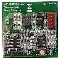
MCP1631RD-MCC1 Microchip Technology, MCP1631RD-MCC1 Datasheet - Page 266

MCP1631RD-MCC1
Manufacturer Part Number
MCP1631RD-MCC1
Description
REFERENCE DESIGN FOR MCP1631HV
Manufacturer
Microchip Technology
Type
Battery Managementr
Datasheets
1.MCP1631VHVT-330EST.pdf
(34 pages)
2.MCP1631HV-330EST.pdf
(54 pages)
3.MCP1631RD-MCC2.pdf
(20 pages)
4.MCP1631RD-MCC2.pdf
(328 pages)
5.MCP1631RD-MCC1.pdf
(28 pages)
Specifications of MCP1631RD-MCC1
Main Purpose
Power Management, Battery Charger
Embedded
Yes, MCU, 8-Bit
Utilized Ic / Part
MCP1631HV, PIC16F883
Primary Attributes
1 ~ 2 Cell- Li-Ion, 1 ~ 4 Cell- NiCd/NiMH
Secondary Attributes
Status LEDs
Supported Devices
MCP1631HV, PIC16F883 Device Type
Tool / Board Applications
Power Management-Battery Management
Development Tool Type
Reference Design
Input Voltage
5.5 V to 16 V
Product
Power Management Modules
Mcu Supported Families
MCP1631HV/PIC16F883 Family
Silicon Manufacturer
Microchip
Silicon Core Number
MCP1631HV
Kit Application Type
Reference Design
Application Sub Type
Battery Charger
Kit Contents
Board Only
Lead Free Status / RoHS Status
Lead free / RoHS Compliant
For Use With/related Products
MCP1631HV, PIC16F883
Lead Free Status / RoHS Status
Lead free / RoHS Compliant
- MCP1631VHVT-330EST PDF datasheet
- MCP1631HV-330EST PDF datasheet #2
- MCP1631RD-MCC2 PDF datasheet #3
- MCP1631RD-MCC2 PDF datasheet #4
- MCP1631RD-MCC1 PDF datasheet #5
- Current page: 266 of 328
- Download datasheet (6Mb)
PIC16F882/883/884/886/887
TABLE 17-11: PIC16F883/884/886/887 A/D CONVERSION REQUIREMENTS
DS41291F-page 264
Standard Operating Conditions (unless otherwise stated)
Operating temperature
AD130* T
AD131 T
AD132* T
AD133* T
AD134 T
Note 1:
Param
No.
2:
*
† Data in “Typ” column is at 5.0V, 25°C unless otherwise stated. These parameters are for design guidance
Sym.
AD
CNV
ACQ
AMP
GO
These parameters are characterized but not tested.
only and are not tested.
ADRESH and ADRESL registers may be read on the following T
See Section 9.3 “A/D Acquisition Requirements” for minimum conditions.
A/D Clock Period
A/D Internal RC
Oscillator Period
Conversion Time
(not including
Acquisition Time)
Acquisition Time
Amplifier Settling Time
Q4 to A/D Clock Start
Characteristic
-40°C ≤ T
(1)
A
≤ +125°C
Min.
1.6
3.0
3.0
1.6
—
—
—
—
T
OSC
T
Typ†
OSC
11.5
6.0
4.0
/2 + T
—
—
11
—
/2
CY
Max. Units
9.0
9.0
9.0
6.0
—
—
—
—
5
T
μs
μs
μs
μs
μs
μs
—
—
AD
CY
T
T
ADCS<1:0> = 11 (ADRC mode)
At V
At V
Set GO/DONE bit to new data in A/D
Result register
If the A/D clock source is selected as
RC, a time of T
A/D clock starts. This allows the SLEEP
instruction to be executed.
OSC
OSC
cycle.
DD
DD
-based, V
-based, V
= 2.5V
= 5.0V
© 2009 Microchip Technology Inc.
Conditions
REF
REF
CY
≥ 3.0V
is added before the
full range
Related parts for MCP1631RD-MCC1
Image
Part Number
Description
Manufacturer
Datasheet
Request
R

Part Number:
Description:
REFERENCE DESIGN MCP1631HV
Manufacturer:
Microchip Technology
Datasheet:

Part Number:
Description:
REF DES BATT CHARG OR LED DRIVER
Manufacturer:
Microchip Technology
Datasheet:

Part Number:
Description:
Manufacturer:
Microchip Technology Inc.
Datasheet:

Part Number:
Description:
Manufacturer:
Microchip Technology Inc.
Datasheet:

Part Number:
Description:
Manufacturer:
Microchip Technology Inc.
Datasheet:

Part Number:
Description:
Manufacturer:
Microchip Technology Inc.
Datasheet:

Part Number:
Description:
Manufacturer:
Microchip Technology Inc.
Datasheet:

Part Number:
Description:
Manufacturer:
Microchip Technology Inc.
Datasheet:

Part Number:
Description:
Manufacturer:
Microchip Technology Inc.
Datasheet:

Part Number:
Description:
Manufacturer:
Microchip Technology Inc.
Datasheet:


