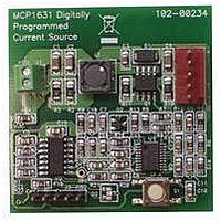
MCP1631RD-MCC1 Microchip Technology, MCP1631RD-MCC1 Datasheet - Page 179

MCP1631RD-MCC1
Manufacturer Part Number
MCP1631RD-MCC1
Description
REFERENCE DESIGN FOR MCP1631HV
Manufacturer
Microchip Technology
Type
Battery Managementr
Datasheets
1.MCP1631VHVT-330EST.pdf
(34 pages)
2.MCP1631HV-330EST.pdf
(54 pages)
3.MCP1631RD-MCC2.pdf
(20 pages)
4.MCP1631RD-MCC2.pdf
(328 pages)
5.MCP1631RD-MCC1.pdf
(28 pages)
Specifications of MCP1631RD-MCC1
Main Purpose
Power Management, Battery Charger
Embedded
Yes, MCU, 8-Bit
Utilized Ic / Part
MCP1631HV, PIC16F883
Primary Attributes
1 ~ 2 Cell- Li-Ion, 1 ~ 4 Cell- NiCd/NiMH
Secondary Attributes
Status LEDs
Supported Devices
MCP1631HV, PIC16F883 Device Type
Tool / Board Applications
Power Management-Battery Management
Development Tool Type
Reference Design
Input Voltage
5.5 V to 16 V
Product
Power Management Modules
Mcu Supported Families
MCP1631HV/PIC16F883 Family
Silicon Manufacturer
Microchip
Silicon Core Number
MCP1631HV
Kit Application Type
Reference Design
Application Sub Type
Battery Charger
Kit Contents
Board Only
Lead Free Status / RoHS Status
Lead free / RoHS Compliant
For Use With/related Products
MCP1631HV, PIC16F883
Lead Free Status / RoHS Status
Lead free / RoHS Compliant
- MCP1631VHVT-330EST PDF datasheet
- MCP1631HV-330EST PDF datasheet #2
- MCP1631RD-MCC2 PDF datasheet #3
- MCP1631RD-MCC2 PDF datasheet #4
- MCP1631RD-MCC1 PDF datasheet #5
- Current page: 179 of 328
- Download datasheet (6Mb)
12.5
The EUSART WILL remain active during Sleep only in
the Synchronous Slave mode. All other modes require
the system clock and therefore cannot generate the
necessary signals to run the Transmit or Receive Shift
registers during Sleep.
Synchronous Slave mode uses an externally generated
clock to run the Transmit and Receive Shift registers.
12.5.1
To receive during Sleep, all the following conditions
must be met before entering Sleep mode:
• RCSTA and TXSTA Control registers must be
• If interrupts are desired, set the RCIE bit of the
• The RCIF interrupt flag must be cleared by read-
Upon entering Sleep mode, the device will be ready to
accept data and clocks on the RX/DT and TX/CK pins,
respectively. When the data word has been completely
clocked in by the external device, the RCIF interrupt
flag bit of the PIR1 register will be set. Thereby, waking
the processor from Sleep.
Upon waking from Sleep, the instruction following the
SLEEP instruction will be executed. If the GIE global
interrupt enable bit of the INTCON register is also set,
then the Interrupt Service Routine at address 004h will
be called.
© 2009 Microchip Technology Inc.
configured for Synchronous Slave Reception (see
Section 12.4.2.4 “Synchronous Slave
Reception Set-up:”).
PIE1 register and the GIE and PEIE bits of the
INTCON register.
ing RCREG to unload any pending characters in
the receive buffer.
EUSART Operation During Sleep
SYNCHRONOUS RECEIVE DURING
SLEEP
PIC16F882/883/884/886/887
12.5.2
To transmit during Sleep, all the following conditions
must be met before entering Sleep mode:
• RCSTA and TXSTA Control registers must be
• The TXIF interrupt flag must be cleared by writing
9.
• Interrupt enable bits TXIE of the PIE1 register and
Upon entering Sleep mode, the device will be ready to
accept clocks on TX/CK pin and transmit data on the
RX/DT pin. When the data word in the TSR has been
completely clocked out by the external device, the
pending byte in the TXREG will transfer to the TSR and
the TXIF flag will be set. Thereby, waking the processor
from Sleep. At this point, the TXREG is available to
accept another character for transmission, which will
clear the TXIF flag.
Upon waking from Sleep, the instruction following the
SLEEP instruction will be executed. If the GIE global
interrupt enable bit is also set then the Interrupt Service
Routine at address 0004h will be called.
configured for Synchronous Slave Transmission
(see Section 12.4.2.2 “Synchronous Slave
Transmission Set-up:”).
the output data to the TXREG, thereby filling the
TSR and transmit buffer.
PEIE of the INTCON register must set.
If interrupts are desired, set the TXIE bit of the
PIE1 register and the PEIE bit of the INTCON
register.
SYNCHRONOUS TRANSMIT
DURING SLEEP
DS41291F-page 177
Related parts for MCP1631RD-MCC1
Image
Part Number
Description
Manufacturer
Datasheet
Request
R

Part Number:
Description:
REFERENCE DESIGN MCP1631HV
Manufacturer:
Microchip Technology
Datasheet:

Part Number:
Description:
REF DES BATT CHARG OR LED DRIVER
Manufacturer:
Microchip Technology
Datasheet:

Part Number:
Description:
Manufacturer:
Microchip Technology Inc.
Datasheet:

Part Number:
Description:
Manufacturer:
Microchip Technology Inc.
Datasheet:

Part Number:
Description:
Manufacturer:
Microchip Technology Inc.
Datasheet:

Part Number:
Description:
Manufacturer:
Microchip Technology Inc.
Datasheet:

Part Number:
Description:
Manufacturer:
Microchip Technology Inc.
Datasheet:

Part Number:
Description:
Manufacturer:
Microchip Technology Inc.
Datasheet:

Part Number:
Description:
Manufacturer:
Microchip Technology Inc.
Datasheet:

Part Number:
Description:
Manufacturer:
Microchip Technology Inc.
Datasheet:


