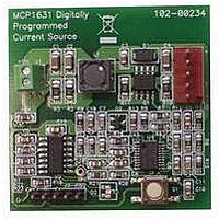
MCP1631RD-MCC1 Microchip Technology, MCP1631RD-MCC1 Datasheet - Page 224

MCP1631RD-MCC1
Manufacturer Part Number
MCP1631RD-MCC1
Description
REFERENCE DESIGN FOR MCP1631HV
Manufacturer
Microchip Technology
Type
Battery Managementr
Datasheets
1.MCP1631VHVT-330EST.pdf
(34 pages)
2.MCP1631HV-330EST.pdf
(54 pages)
3.MCP1631RD-MCC2.pdf
(20 pages)
4.MCP1631RD-MCC2.pdf
(328 pages)
5.MCP1631RD-MCC1.pdf
(28 pages)
Specifications of MCP1631RD-MCC1
Main Purpose
Power Management, Battery Charger
Embedded
Yes, MCU, 8-Bit
Utilized Ic / Part
MCP1631HV, PIC16F883
Primary Attributes
1 ~ 2 Cell- Li-Ion, 1 ~ 4 Cell- NiCd/NiMH
Secondary Attributes
Status LEDs
Supported Devices
MCP1631HV, PIC16F883 Device Type
Tool / Board Applications
Power Management-Battery Management
Development Tool Type
Reference Design
Input Voltage
5.5 V to 16 V
Product
Power Management Modules
Mcu Supported Families
MCP1631HV/PIC16F883 Family
Silicon Manufacturer
Microchip
Silicon Core Number
MCP1631HV
Kit Application Type
Reference Design
Application Sub Type
Battery Charger
Kit Contents
Board Only
Lead Free Status / RoHS Status
Lead free / RoHS Compliant
For Use With/related Products
MCP1631HV, PIC16F883
Lead Free Status / RoHS Status
Lead free / RoHS Compliant
- MCP1631VHVT-330EST PDF datasheet
- MCP1631HV-330EST PDF datasheet #2
- MCP1631RD-MCC2 PDF datasheet #3
- MCP1631RD-MCC2 PDF datasheet #4
- MCP1631RD-MCC1 PDF datasheet #5
- Current page: 224 of 328
- Download datasheet (6Mb)
PIC16F882/883/884/886/887
FIGURE 14-8:
TABLE 14-6:
DS41291F-page 222
INTCON
PIE1
PIE2
PIR1
PIR2
Legend:
INSTRUCTION FLOW
(INTCON<7>)
(INTCON<1>)
CLKOUT
Name
Note 1: INTF flag is sampled here (every Q1).
Instruction
Executed
Instruction
Fetched
INTF flag
INT pin
GIE bit
OSC1
2: Asynchronous interrupt latency = 3-4 T
3: CLKOUT is available only in INTOSC and RC Oscillator modes.
4: For minimum width of INT pulse, refer to AC specifications in Section 17.0 “Electrical Specifications”.
5: INTF is enabled to be set any time during the Q4-Q1 cycles.
PC
x = unknown, u = unchanged, — = unimplemented read as ‘0’, q = value depends upon condition.
Shaded cells are not used by the Interrupt module.
(3)
is the same whether Inst (PC) is a single cycle or a 2-cycle instruction.
OSFIE
OSFIF
Bit 7
GIE
—
—
SUMMARY OF INTERRUPT REGISTERS
Q1
Inst (PC – 1)
Inst (PC)
(1)
INT PIN INTERRUPT TIMING
Q2
PC
PEIE
ADIE
C2IE
ADIF
Bit 6
C2IF
(4)
Q3
Q4
(5)
RCIE
RCIF
Bit 5
C1IE
C1IF
T0IE
Q1
Inst (PC + 1)
Inst (PC)
Q2
(1)
INTE
EEIE
Bit 4
TXIE
TXIF
EEIF
PC + 1
Q3
CY
. Synchronous latency = 3 T
Q4
SSPIE
BCLIE
SSPIF
BCLIF
RBIE
Bit 3
Interrupt Latency
Q1
Dummy Cycle
ULPWUIE
ULPWUIF
Q2
CCP1IE
CCP1IF
PC + 1
Bit 2
T0IF
—
Q3
Q4
(2)
TMR2IE
TMR2IF
Bit 1
INTF
CY
—
—
, where T
Q1
Dummy Cycle
Inst (0004h)
Q2
TMR1IE
CCP2IE
TMR1IF
CCP2IF
0004h
Bit 0
RBIF
CY
= instruction cycle time. Latency
Q3
© 2009 Microchip Technology Inc.
Q4
0000 000x
-000 0000
0000 00-0
-000 0000
0000 00-0
POR, BOR
Value on
Q1
Inst (0005h)
Q2
Inst (0004h)
0005h
0000 000x
-000 0000
0000 00-0
-000 0000
0000 00-0
Q3
Value on
all other
Resets
Q4
Related parts for MCP1631RD-MCC1
Image
Part Number
Description
Manufacturer
Datasheet
Request
R

Part Number:
Description:
REFERENCE DESIGN MCP1631HV
Manufacturer:
Microchip Technology
Datasheet:

Part Number:
Description:
REF DES BATT CHARG OR LED DRIVER
Manufacturer:
Microchip Technology
Datasheet:

Part Number:
Description:
Manufacturer:
Microchip Technology Inc.
Datasheet:

Part Number:
Description:
Manufacturer:
Microchip Technology Inc.
Datasheet:

Part Number:
Description:
Manufacturer:
Microchip Technology Inc.
Datasheet:

Part Number:
Description:
Manufacturer:
Microchip Technology Inc.
Datasheet:

Part Number:
Description:
Manufacturer:
Microchip Technology Inc.
Datasheet:

Part Number:
Description:
Manufacturer:
Microchip Technology Inc.
Datasheet:

Part Number:
Description:
Manufacturer:
Microchip Technology Inc.
Datasheet:

Part Number:
Description:
Manufacturer:
Microchip Technology Inc.
Datasheet:


