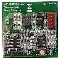
MCP1631RD-MCC1 Microchip Technology, MCP1631RD-MCC1 Datasheet - Page 116

MCP1631RD-MCC1
Manufacturer Part Number
MCP1631RD-MCC1
Description
REFERENCE DESIGN FOR MCP1631HV
Manufacturer
Microchip Technology
Type
Battery Managementr
Datasheets
1.MCP1631VHVT-330EST.pdf
(34 pages)
2.MCP1631HV-330EST.pdf
(54 pages)
3.MCP1631RD-MCC2.pdf
(20 pages)
4.MCP1631RD-MCC2.pdf
(328 pages)
5.MCP1631RD-MCC1.pdf
(28 pages)
Specifications of MCP1631RD-MCC1
Main Purpose
Power Management, Battery Charger
Embedded
Yes, MCU, 8-Bit
Utilized Ic / Part
MCP1631HV, PIC16F883
Primary Attributes
1 ~ 2 Cell- Li-Ion, 1 ~ 4 Cell- NiCd/NiMH
Secondary Attributes
Status LEDs
Supported Devices
MCP1631HV, PIC16F883 Device Type
Tool / Board Applications
Power Management-Battery Management
Development Tool Type
Reference Design
Input Voltage
5.5 V to 16 V
Product
Power Management Modules
Mcu Supported Families
MCP1631HV/PIC16F883 Family
Silicon Manufacturer
Microchip
Silicon Core Number
MCP1631HV
Kit Application Type
Reference Design
Application Sub Type
Battery Charger
Kit Contents
Board Only
Lead Free Status / RoHS Status
Lead free / RoHS Compliant
For Use With/related Products
MCP1631HV, PIC16F883
Lead Free Status / RoHS Status
Lead free / RoHS Compliant
- MCP1631VHVT-330EST PDF datasheet
- MCP1631HV-330EST PDF datasheet #2
- MCP1631RD-MCC2 PDF datasheet #3
- MCP1631RD-MCC2 PDF datasheet #4
- MCP1631RD-MCC1 PDF datasheet #5
- Current page: 116 of 328
- Download datasheet (6Mb)
PIC16F882/883/884/886/887
10.1.2
To read a data memory location, the user must write the
address to the EEADR register, clear the EEPGD
control bit of the EECON1 register, and then set control
bit RD. The data is available at the very next cycle, in
the EEDAT register; therefore, it can be read in the next
instruction. EEDAT will hold this value until another
read or until it is written to by the user (during a write
operation).
EXAMPLE 10-1:
EXAMPLE 10-2:
DS41291F-page 114
BANKSEL EEADR
MOVLW
MOVWF
BANKSEL EECON1
BCF
BSF
BANKSEL EEDAT
MOVF
BCF
BANKSEL EEADR
MOVLW
MOVWF
MOVLW
MOVWF
BANKSEL EECON1
BCF
BSF
BCF
BTFSC
GOTO
MOVLW
MOVWF
MOVLW
MOVWF
BSF
BSF
SLEEP
BCF
BCF
BCF
DATA_EE_ADDR
EEADR
EECON1, EEPGD ;Point to DATA memory
EECON1, RD
EEDAT, W
STATUS, RP1
READING THE DATA EEPROM
MEMORY
DATA_EE_ADDR
EEADR
DATA_EE_DATA
EEDAT
EECON1, EEPGD
EECON1, WREN
INTCON, GIE
INTCON, GIE
$-2
55h
EECON2
AAh
EECON2
EECON1, WR
INTCON, GIE
EECON1, WREN
STATUS, RP0
STATUS, RP1
DATA EEPROM READ
DATA EEPROM WRITE
;
;
;Data Memory
;Address to read
;
;EE Read
;
;W = EEDAT
;Bank 0
;
;
;Data Memory Address to write
;
;Data Memory Value to write
;
;Point to DATA memory
;Enable writes
;Disable INTs.
;SEE AN576
;
;Write 55h
;
;Write AAh
;Set WR bit to begin write
;Enable INTs.
;Wait for interrupt to signal write complete
;Disable writes
;Bank 0
10.1.3
To write an EEPROM data location, the user must first
write the address to the EEADR register and the data
to the EEDAT register. Then the user must follow a
specific sequence to initiate the write for each byte.
The write will not initiate if the above sequence is not
followed exactly (write 55h to EECON2, write AAh to
EECON2, then set WR bit) for each byte. Interrupts
should be disabled during this code segment.
Additionally, the WREN bit in EECON1 must be set to
enable write. This mechanism prevents accidental
writes to data EEPROM due to errant (unexpected)
code execution (i.e., lost programs). The user should
keep the WREN bit clear at all times, except when
updating EEPROM. The WREN bit is not cleared
by hardware.
After a write sequence has been initiated, clearing the
WREN bit will not affect this write cycle. The WR bit will
be inhibited from being set unless the WREN bit is set.
At the completion of the write cycle, the WR bit is
cleared in hardware and the EE Write Complete
Interrupt Flag bit (EEIF) is set. The user can either
enable this interrupt or poll this bit. EEIF must be
cleared by software.
WRITING TO THE DATA EEPROM
MEMORY
© 2009 Microchip Technology Inc.
Related parts for MCP1631RD-MCC1
Image
Part Number
Description
Manufacturer
Datasheet
Request
R

Part Number:
Description:
REFERENCE DESIGN MCP1631HV
Manufacturer:
Microchip Technology
Datasheet:

Part Number:
Description:
REF DES BATT CHARG OR LED DRIVER
Manufacturer:
Microchip Technology
Datasheet:

Part Number:
Description:
Manufacturer:
Microchip Technology Inc.
Datasheet:

Part Number:
Description:
Manufacturer:
Microchip Technology Inc.
Datasheet:

Part Number:
Description:
Manufacturer:
Microchip Technology Inc.
Datasheet:

Part Number:
Description:
Manufacturer:
Microchip Technology Inc.
Datasheet:

Part Number:
Description:
Manufacturer:
Microchip Technology Inc.
Datasheet:

Part Number:
Description:
Manufacturer:
Microchip Technology Inc.
Datasheet:

Part Number:
Description:
Manufacturer:
Microchip Technology Inc.
Datasheet:

Part Number:
Description:
Manufacturer:
Microchip Technology Inc.
Datasheet:


