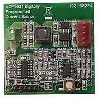
MCP1631RD-MCC1 Microchip Technology, MCP1631RD-MCC1 Datasheet - Page 182

MCP1631RD-MCC1
Manufacturer Part Number
MCP1631RD-MCC1
Description
REFERENCE DESIGN FOR MCP1631HV
Manufacturer
Microchip Technology
Type
Battery Managementr
Datasheets
1.MCP1631VHVT-330EST.pdf
(34 pages)
2.MCP1631HV-330EST.pdf
(54 pages)
3.MCP1631RD-MCC2.pdf
(20 pages)
4.MCP1631RD-MCC2.pdf
(328 pages)
5.MCP1631RD-MCC1.pdf
(28 pages)
Specifications of MCP1631RD-MCC1
Main Purpose
Power Management, Battery Charger
Embedded
Yes, MCU, 8-Bit
Utilized Ic / Part
MCP1631HV, PIC16F883
Primary Attributes
1 ~ 2 Cell- Li-Ion, 1 ~ 4 Cell- NiCd/NiMH
Secondary Attributes
Status LEDs
Supported Devices
MCP1631HV, PIC16F883 Device Type
Tool / Board Applications
Power Management-Battery Management
Development Tool Type
Reference Design
Input Voltage
5.5 V to 16 V
Product
Power Management Modules
Mcu Supported Families
MCP1631HV/PIC16F883 Family
Silicon Manufacturer
Microchip
Silicon Core Number
MCP1631HV
Kit Application Type
Reference Design
Application Sub Type
Battery Charger
Kit Contents
Board Only
Lead Free Status / RoHS Status
Lead free / RoHS Compliant
For Use With/related Products
MCP1631HV, PIC16F883
Lead Free Status / RoHS Status
Lead free / RoHS Compliant
- MCP1631VHVT-330EST PDF datasheet
- MCP1631HV-330EST PDF datasheet #2
- MCP1631RD-MCC2 PDF datasheet #3
- MCP1631RD-MCC2 PDF datasheet #4
- MCP1631RD-MCC1 PDF datasheet #5
- Current page: 182 of 328
- Download datasheet (6Mb)
PIC16F882/883/884/886/887
REGISTER 13-1:
DS41291F-page 180
bit 7
Legend:
R = Readable bit
-n = Value at POR
bit 7
bit 6
bit 5
bit 4
bit 3
bit 2
bit 1
bit 0
R/W-0
SMP
SMP: Sample bit
SPI Master mode:
1 = Input data sampled at end of data output time
0 = Input data sampled at middle of data output time
SPI Slave mode:
SMP must be cleared when SPI is used in Slave mode
In I
1 = Slew rate control disabled for standard speed mode (100 kHz and 1 MHz)
0 = Slew rate control enabled for high speed mode (400 kHz)
CKE: SPI Clock Edge Select bit
CKP = 0:
1 = Data transmitted on rising edge of SCK
0 = Data transmitted on falling edge of SCK
CKP = 1:
1 = Data transmitted on falling edge of SCK
0 = Data transmitted on rising edge of SCK
D/A: Data/Address bit (I
1 = Indicates that the last byte received or transmitted was data
0 = Indicates that the last byte received or transmitted was address
P: Stop bit
(I
1 = Indicates that a Stop bit has been detected last (this bit is ‘0’ on Reset)
0 = Stop bit was not detected last
S: Start bit
(I
1 = Indicates that a Start bit has been detected last (this bit is ‘0’ on Reset)
0 = Start bit was not detected last
R/W: Read/Write bit information (I
This bit holds the R/W bit information following the last address match. This bit is only valid from the address match to
the next Start bit, Stop bit, or not ACK bit.
In I
1 = Read
0 = Write
In I
1 = Transmit is in progress
0 = Transmit is not in progress
UA: Update Address bit (10-bit I
1 = Indicates that the user needs to update the address in the SSPADD register
0 = Address does not need to be updated
BF: Buffer Full Status bit
Receive (SPI and I
1 = Receive complete, SSPBUF is full
0 = Receive not complete, SSPBUF is empty
Transmit (I
1 = Data transmit in progress (does not include the ACK and Stop bits), SSPBUF is full
0 = Data transmit complete (does not include the ACK and Stop bits), SSPBUF is empty
2
2
C mode only. This bit is cleared when the MSSP module is disabled, SSPEN is cleared.)
C mode only. This bit is cleared when the MSSP module is disabled, SSPEN is cleared.)
2
2
2
C Master or Slave mode:
C Slave mode:
C Master mode:
R/W-0
CKE
OR-ing this bit with SEN, RSEN, PEN, RCEN, or ACKEN will indicate if the MSSP is in Idle mode.
SSPSTAT: SSP STATUS REGISTER
2
C mode only):
W = Writable bit
‘1’ = Bit is set
2
C modes):
R-0
D/A
2
C mode only)
2
C mode only)
2
C mode only)
R-0
P
U = Unimplemented bit, read as ‘0’
‘0’ = Bit is cleared
R-0
S
R/W
R-0
© 2009 Microchip Technology Inc.
x = Bit is unknown
R-0
UA
R-0
BF
bit 0
Related parts for MCP1631RD-MCC1
Image
Part Number
Description
Manufacturer
Datasheet
Request
R

Part Number:
Description:
REFERENCE DESIGN MCP1631HV
Manufacturer:
Microchip Technology
Datasheet:

Part Number:
Description:
REF DES BATT CHARG OR LED DRIVER
Manufacturer:
Microchip Technology
Datasheet:

Part Number:
Description:
Manufacturer:
Microchip Technology Inc.
Datasheet:

Part Number:
Description:
Manufacturer:
Microchip Technology Inc.
Datasheet:

Part Number:
Description:
Manufacturer:
Microchip Technology Inc.
Datasheet:

Part Number:
Description:
Manufacturer:
Microchip Technology Inc.
Datasheet:

Part Number:
Description:
Manufacturer:
Microchip Technology Inc.
Datasheet:

Part Number:
Description:
Manufacturer:
Microchip Technology Inc.
Datasheet:

Part Number:
Description:
Manufacturer:
Microchip Technology Inc.
Datasheet:

Part Number:
Description:
Manufacturer:
Microchip Technology Inc.
Datasheet:


