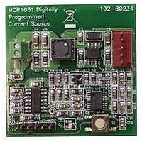
MCP1631RD-MCC1 Microchip Technology, MCP1631RD-MCC1 Datasheet - Page 265

MCP1631RD-MCC1
Manufacturer Part Number
MCP1631RD-MCC1
Description
REFERENCE DESIGN FOR MCP1631HV
Manufacturer
Microchip Technology
Type
Battery Managementr
Datasheets
1.MCP1631VHVT-330EST.pdf
(34 pages)
2.MCP1631HV-330EST.pdf
(54 pages)
3.MCP1631RD-MCC2.pdf
(20 pages)
4.MCP1631RD-MCC2.pdf
(328 pages)
5.MCP1631RD-MCC1.pdf
(28 pages)
Specifications of MCP1631RD-MCC1
Main Purpose
Power Management, Battery Charger
Embedded
Yes, MCU, 8-Bit
Utilized Ic / Part
MCP1631HV, PIC16F883
Primary Attributes
1 ~ 2 Cell- Li-Ion, 1 ~ 4 Cell- NiCd/NiMH
Secondary Attributes
Status LEDs
Supported Devices
MCP1631HV, PIC16F883 Device Type
Tool / Board Applications
Power Management-Battery Management
Development Tool Type
Reference Design
Input Voltage
5.5 V to 16 V
Product
Power Management Modules
Mcu Supported Families
MCP1631HV/PIC16F883 Family
Silicon Manufacturer
Microchip
Silicon Core Number
MCP1631HV
Kit Application Type
Reference Design
Application Sub Type
Battery Charger
Kit Contents
Board Only
Lead Free Status / RoHS Status
Lead free / RoHS Compliant
For Use With/related Products
MCP1631HV, PIC16F883
Lead Free Status / RoHS Status
Lead free / RoHS Compliant
- MCP1631VHVT-330EST PDF datasheet
- MCP1631HV-330EST PDF datasheet #2
- MCP1631RD-MCC2 PDF datasheet #3
- MCP1631RD-MCC2 PDF datasheet #4
- MCP1631RD-MCC1 PDF datasheet #5
- Current page: 265 of 328
- Download datasheet (6Mb)
TABLE 17-10: PIC16F883/884/886/887 A/D CONVERTER (ADC) CHARACTERISTICS
© 2009 Microchip Technology Inc.
Standard Operating Conditions (unless otherwise stated)
Operating temperature
AD01
AD02
AD03
AD04
AD07
AD06
AD06A
AD07
AD08
AD09* I
Note 1:
Param
No.
2:
3:
4:
*
† Data in “Typ” column is at 5.0V, 25°C unless otherwise stated. These parameters are for design guidance
N
E
E
E
E
V
V
Z
Sym.
REF
REF
AIN
AIN
IL
DL
OFF
GN
R
These parameters are characterized but not tested.
only and are not tested.
Total Absolute Error includes integral, differential, offset and gain errors.
The A/D conversion result never decreases with an increase in the input voltage and has no missing
codes.
ADC V
When ADC is off, it will not consume any current other than leakage current. The power-down current
specification includes any such leakage from the ADC module.
Resolution
Integral Error
Differential Error
Offset Error
Gain Error
Reference Voltage
Full-Scale Range
Recommended
Impedance of Analog
Voltage Source
V
REF
REF
Characteristic
Input Current
is from external V
-40°C ≤ T
(3)
(3)
A
≤ +125°C
REF
Min.
V
2.2
2.7
10
—
—
—
—
—
—
or V
0
SS
PIC16F882/883/884/886/887
DD
pin, whichever is selected as reference input.
Typ†
+1.5
—
—
—
—
—
—
—
—
—
10 bits
Max.
V
1000
+3.0
V
±1
±1
±1
10
50
—
REF
DD
Units
LSb V
LSb No missing codes to 10 bits
LSb V
LSb V
kΩ
μA
μA
bit
V
V
V
Absolute minimum to ensure 1 LSb
accuracy
During V
Based on differential of V
During A/D conversion cycle.
REF
REF
REF
REF
= 5.12V
= 5.12V
= 5.12V
= 5.12V
AIN
acquisition.
Conditions
DS41291F-page 263
HOLD
to V
AIN
.
Related parts for MCP1631RD-MCC1
Image
Part Number
Description
Manufacturer
Datasheet
Request
R

Part Number:
Description:
REFERENCE DESIGN MCP1631HV
Manufacturer:
Microchip Technology
Datasheet:

Part Number:
Description:
REF DES BATT CHARG OR LED DRIVER
Manufacturer:
Microchip Technology
Datasheet:

Part Number:
Description:
Manufacturer:
Microchip Technology Inc.
Datasheet:

Part Number:
Description:
Manufacturer:
Microchip Technology Inc.
Datasheet:

Part Number:
Description:
Manufacturer:
Microchip Technology Inc.
Datasheet:

Part Number:
Description:
Manufacturer:
Microchip Technology Inc.
Datasheet:

Part Number:
Description:
Manufacturer:
Microchip Technology Inc.
Datasheet:

Part Number:
Description:
Manufacturer:
Microchip Technology Inc.
Datasheet:

Part Number:
Description:
Manufacturer:
Microchip Technology Inc.
Datasheet:

Part Number:
Description:
Manufacturer:
Microchip Technology Inc.
Datasheet:


