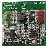
MCP1631RD-MCC1 Microchip Technology, MCP1631RD-MCC1 Datasheet - Page 203

MCP1631RD-MCC1
Manufacturer Part Number
MCP1631RD-MCC1
Description
REFERENCE DESIGN FOR MCP1631HV
Manufacturer
Microchip Technology
Type
Battery Managementr
Datasheets
1.MCP1631VHVT-330EST.pdf
(34 pages)
2.MCP1631HV-330EST.pdf
(54 pages)
3.MCP1631RD-MCC2.pdf
(20 pages)
4.MCP1631RD-MCC2.pdf
(328 pages)
5.MCP1631RD-MCC1.pdf
(28 pages)
Specifications of MCP1631RD-MCC1
Main Purpose
Power Management, Battery Charger
Embedded
Yes, MCU, 8-Bit
Utilized Ic / Part
MCP1631HV, PIC16F883
Primary Attributes
1 ~ 2 Cell- Li-Ion, 1 ~ 4 Cell- NiCd/NiMH
Secondary Attributes
Status LEDs
Supported Devices
MCP1631HV, PIC16F883 Device Type
Tool / Board Applications
Power Management-Battery Management
Development Tool Type
Reference Design
Input Voltage
5.5 V to 16 V
Product
Power Management Modules
Mcu Supported Families
MCP1631HV/PIC16F883 Family
Silicon Manufacturer
Microchip
Silicon Core Number
MCP1631HV
Kit Application Type
Reference Design
Application Sub Type
Battery Charger
Kit Contents
Board Only
Lead Free Status / RoHS Status
Lead free / RoHS Compliant
For Use With/related Products
MCP1631HV, PIC16F883
Lead Free Status / RoHS Status
Lead free / RoHS Compliant
- MCP1631VHVT-330EST PDF datasheet
- MCP1631HV-330EST PDF datasheet #2
- MCP1631RD-MCC2 PDF datasheet #3
- MCP1631RD-MCC2 PDF datasheet #4
- MCP1631RD-MCC1 PDF datasheet #5
- Current page: 203 of 328
- Download datasheet (6Mb)
13.4.10
An Acknowledge sequence is enabled by setting the
Acknowledge Sequence Enable bit, ACKEN (SSPCON2
register). When this bit is set, the SCL pin is pulled low
and the contents of the Acknowledge Data bit (ACKDT)
is presented on the SDA pin. If the user wishes to gener-
ate an Acknowledge, then the ACKDT bit should be
cleared. If not, the user should set the ACKDT bit before
starting an Acknowledge sequence. The Baud Rate
Generator then counts for one rollover period (T
the SCL pin is de-asserted (pulled high). When the SCL
pin is sampled high (clock arbitration), the Baud Rate
Generator counts for T
low. Following this, the ACKEN bit is automatically
cleared, the Baud Rate Generator is turned off and the
MSSP module then goes into Idle mode (Figure 13-17).
13.4.10.1
If the user writes the SSPBUF when an Acknowledge
sequence is in progress, then WCOL is set and the
contents of the buffer are unchanged (the write doesn’t
occur).
FIGURE 13-17:
© 2009 Microchip Technology Inc.
Note: T
ACKNOWLEDGE SEQUENCE TIMING
WCOL Status Flag
SSPIF
BRG
Acknowledge sequence starts here,
SDA
SCL
= one Baud Rate Generator period.
BRG
ACKNOWLEDGE SEQUENCE WAVEFORM
Set SSPIF at the end
of receive
. The SCL pin is then pulled
ACKEN = 1, ACKDT = 0
Write to SSPCON2
8
D0
BRG
PIC16F882/883/884/886/887
) and
Cleared in
software
T
BRG
ACK
13.4.11
A Stop bit is asserted on the SDA pin at the end of a
receive/transmit by setting the Stop Sequence Enable
bit, PEN (SSPCON2 register). At the end of a receive/
transmit, the SCL line is held low after the falling edge
of the ninth clock. When the PEN bit is set, the master
will assert the SDA line low. When the SDA line is sam-
pled low, the Baud Rate Generator is reloaded and
counts down to 0. When the Baud Rate Generator
times out, the SCL pin will be brought high, and one
T
SDA pin will be de-asserted. When the SDA pin is sam-
pled high while SCL is high, the P bit (SSPSTAT regis-
ter) is set. A T
SSPIF bit is set (Figure 13-18).
13.4.11.1
If the user writes the SSPBUF when a Stop sequence
is in progress, then the WCOL bit is set and the
contents of the buffer are unchanged (the write doesn’t
occur).
BRG
T
BRG
9
(Baud Rate Generator rollover count) later, the
Set SSPIF at the end
of Acknowledge sequence
STOP CONDITION TIMING
WCOL Status Flag
BRG
ACKEN automatically cleared
later, the PEN bit is cleared and the
Cleared in
software
DS41291F-page 201
Related parts for MCP1631RD-MCC1
Image
Part Number
Description
Manufacturer
Datasheet
Request
R

Part Number:
Description:
REFERENCE DESIGN MCP1631HV
Manufacturer:
Microchip Technology
Datasheet:

Part Number:
Description:
REF DES BATT CHARG OR LED DRIVER
Manufacturer:
Microchip Technology
Datasheet:

Part Number:
Description:
Manufacturer:
Microchip Technology Inc.
Datasheet:

Part Number:
Description:
Manufacturer:
Microchip Technology Inc.
Datasheet:

Part Number:
Description:
Manufacturer:
Microchip Technology Inc.
Datasheet:

Part Number:
Description:
Manufacturer:
Microchip Technology Inc.
Datasheet:

Part Number:
Description:
Manufacturer:
Microchip Technology Inc.
Datasheet:

Part Number:
Description:
Manufacturer:
Microchip Technology Inc.
Datasheet:

Part Number:
Description:
Manufacturer:
Microchip Technology Inc.
Datasheet:

Part Number:
Description:
Manufacturer:
Microchip Technology Inc.
Datasheet:


