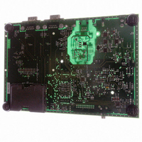
AT91RM3400-DK Atmel, AT91RM3400-DK Datasheet - Page 131

AT91RM3400-DK
Manufacturer Part Number
AT91RM3400-DK
Description
KIT DEV FOR AT91RM3400
Manufacturer
Atmel
Series
AT91SAM Smart ARMr
Type
MCUr
Datasheets
1.AT91RM3400-DK.pdf
(461 pages)
2.AT91RM3400-DK.pdf
(2 pages)
3.AT91RM3400-DK.pdf
(25 pages)
Specifications of AT91RM3400-DK
Contents
Evaluation Board, Software and Documentation
Processor To Be Evaluated
AT91RM3400
Data Bus Width
32 bit
Interface Type
RS-232, USB
For Use With/related Products
AT91RM3400
Lead Free Status / RoHS Status
Contains lead / RoHS non-compliant
- Current page: 131 of 461
- Download datasheet (6Mb)
Main Clock Frequency
Counter
Main Oscillator Bypass
1790A–ATARM–11/03
When enabling the Main Oscillator, the user must initiate the Main Oscillator counter
with a value corresponding to the startup time of the oscillator. This startup time
depends on the crystal frequency connected to the main oscillator. When the MOSCEN
bit and the OSCOUNT are written in CKGR_MOR to enable the Main Oscillator, the
MOSCS bit is cleared and the counter starts counting down on the Slow Clock divided
by 8 from the OSCOUNT value. Since the OSCOUNT value is coded with 8 bits, the
maximum startup time is about 62 ms.
When the counter reaches 0, the MOSCS bit is set, indicating that the Main Clock is
valid. Setting the MOSCS bit in PMC_IMR can trigger an interrupt to the processor on
this event.
The Main Oscillator features a Main Clock frequency counter that provides the quartz
frequency connected to the Main Oscillator. Generally, this value is known by the sys-
tem designer; however, it is useful for the boot program to configure the device with the
correct clock speed, independently of the application.
The Main Clock frequency counter starts incrementing at the Main Clock speed after the
next rising edge of the Slow Clock as soon as the Main Oscillator is stable, i.e., as soon
as the MOSCS bit is set. Then, at the 16th falling edge of Slow Clock, the bit MAINRDY
in CKGR_MCFR (Main Clock Frequency Register) is set and the counter stops count-
ing. Its value can be read in the MAINF field of CKGR_MCFR and gives the number of
Main Clock cycles during 16 periods of Slow Clock, so that the frequency of the crystal
connected on the Main Oscillator can be determined.
The user can input a clock on the device instead of connecting a crystal. In this case, the
user has to provide the external clock signal on the pin XIN. The input characteristics of
the XIN pin under these conditions are given in the product electrical characteristics sec-
tion. The programmer has to be sure not to modify the MOSCEN bit in the Main
Oscillator Register (CKGR_MOR). This bit must remain at 0, its reset value, for the
external clock to operate properly. While this bit is at 0, the pin XIN is tied low to prevent
any internal oscillation regardless of pin connected.
The external clock signal must meet the requirements relating to the power supply
VDDPLL (i.e., between 1.65V and 1.95V) and cannot exceed 50 MHz.
AT91RM3400
131
Related parts for AT91RM3400-DK
Image
Part Number
Description
Manufacturer
Datasheet
Request
R

Part Number:
Description:
DEV KIT FOR AVR/AVR32
Manufacturer:
Atmel
Datasheet:

Part Number:
Description:
INTERVAL AND WIPE/WASH WIPER CONTROL IC WITH DELAY
Manufacturer:
ATMEL Corporation
Datasheet:

Part Number:
Description:
Low-Voltage Voice-Switched IC for Hands-Free Operation
Manufacturer:
ATMEL Corporation
Datasheet:

Part Number:
Description:
MONOLITHIC INTEGRATED FEATUREPHONE CIRCUIT
Manufacturer:
ATMEL Corporation
Datasheet:

Part Number:
Description:
AM-FM Receiver IC U4255BM-M
Manufacturer:
ATMEL Corporation
Datasheet:

Part Number:
Description:
Monolithic Integrated Feature Phone Circuit
Manufacturer:
ATMEL Corporation
Datasheet:

Part Number:
Description:
Multistandard Video-IF and Quasi Parallel Sound Processing
Manufacturer:
ATMEL Corporation
Datasheet:

Part Number:
Description:
High-performance EE PLD
Manufacturer:
ATMEL Corporation
Datasheet:

Part Number:
Description:
8-bit Flash Microcontroller
Manufacturer:
ATMEL Corporation
Datasheet:

Part Number:
Description:
2-Wire Serial EEPROM
Manufacturer:
ATMEL Corporation
Datasheet:


