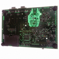
AT91RM3400-DK Atmel, AT91RM3400-DK Datasheet - Page 148

AT91RM3400-DK
Manufacturer Part Number
AT91RM3400-DK
Description
KIT DEV FOR AT91RM3400
Manufacturer
Atmel
Series
AT91SAM Smart ARMr
Type
MCUr
Datasheets
1.AT91RM3400-DK.pdf
(461 pages)
2.AT91RM3400-DK.pdf
(2 pages)
3.AT91RM3400-DK.pdf
(25 pages)
Specifications of AT91RM3400-DK
Contents
Evaluation Board, Software and Documentation
Processor To Be Evaluated
AT91RM3400
Data Bus Width
32 bit
Interface Type
RS-232, USB
For Use With/related Products
AT91RM3400
Lead Free Status / RoHS Status
Contains lead / RoHS non-compliant
- Current page: 148 of 461
- Download datasheet (6Mb)
PMC Clock Generator PLL A Register
Register Name: CKGR_PLLAR
Access Type:
Possible limitations on PLLA input frequencies and multiplier factors should be checked before using the Clock Generator.
• DIVA: Divider A
• PLLACOUNT: PLL A Counter
Specifies the number of Slow Clock cycles before the LOCKA bit is set in PMC_SR after CKGR_PLLAR is written.
• OUTA: PLLA Clock Frequency Range
• MULA: PLL A Multiplier
0 = The PLL A is deactivated.
1 up to 2047 = The PLLA Clock frequency is the PLLA input frequency multiplied by MULA + 1.
148
DIVA
0
1
2 - 255
31
23
15
–
7
0
0
1
1
AT91RM3400
OUTA
OUTA
Read/Write
30
22
14
–
6
0
1
0
1
29
21
13
1
5
Divider Selected
Divider output is 0
Divider is bypassed
Divider output is the Main Clock divided by DIVA.
PLLA Frequency Output Range
80 MHz to 160 MHz
Reserved
150 MHz to 240 MHz
Reserved
28
20
12
–
4
MULA
DIVA
27
19
11
–
3
PLLACOUNT
26
18
10
2
MULA
25
17
9
1
1790A–ATARM–11/03
24
16
8
0
Related parts for AT91RM3400-DK
Image
Part Number
Description
Manufacturer
Datasheet
Request
R

Part Number:
Description:
DEV KIT FOR AVR/AVR32
Manufacturer:
Atmel
Datasheet:

Part Number:
Description:
INTERVAL AND WIPE/WASH WIPER CONTROL IC WITH DELAY
Manufacturer:
ATMEL Corporation
Datasheet:

Part Number:
Description:
Low-Voltage Voice-Switched IC for Hands-Free Operation
Manufacturer:
ATMEL Corporation
Datasheet:

Part Number:
Description:
MONOLITHIC INTEGRATED FEATUREPHONE CIRCUIT
Manufacturer:
ATMEL Corporation
Datasheet:

Part Number:
Description:
AM-FM Receiver IC U4255BM-M
Manufacturer:
ATMEL Corporation
Datasheet:

Part Number:
Description:
Monolithic Integrated Feature Phone Circuit
Manufacturer:
ATMEL Corporation
Datasheet:

Part Number:
Description:
Multistandard Video-IF and Quasi Parallel Sound Processing
Manufacturer:
ATMEL Corporation
Datasheet:

Part Number:
Description:
High-performance EE PLD
Manufacturer:
ATMEL Corporation
Datasheet:

Part Number:
Description:
8-bit Flash Microcontroller
Manufacturer:
ATMEL Corporation
Datasheet:

Part Number:
Description:
2-Wire Serial EEPROM
Manufacturer:
ATMEL Corporation
Datasheet:


