AT91RM3400-DK Atmel, AT91RM3400-DK Datasheet - Page 132
AT91RM3400-DK
Manufacturer Part Number
AT91RM3400-DK
Description
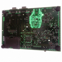
KIT DEV FOR AT91RM3400
Manufacturer
Atmel
Series
AT91SAM Smart ARMr
Type
MCUr
Datasheets
1.AT91RM3400-DK.pdf
(461 pages)
2.AT91RM3400-DK.pdf
(2 pages)
3.AT91RM3400-DK.pdf
(25 pages)
Specifications of AT91RM3400-DK
Contents
Evaluation Board, Software and Documentation
Processor To Be Evaluated
AT91RM3400
Data Bus Width
32 bit
Interface Type
RS-232, USB
For Use With/related Products
AT91RM3400
Lead Free Status / RoHS Status
Contains lead / RoHS non-compliant


Divider and PLL Blocks
PLL Filters
132
AT91RM3400
The Clock Generator features two Divider/PLL Blocks that generates a wide range of
frequencies. Additionally, they provide a 48 MHz signal to the embedded USB device
and/or host ports, regardless of the frequency of the Main Clock.
Figure 40 shows the block diagram of the divider and PLL blocks.
Figure 40. Divider and PLL Blocks Block Diagram
The two PLLs require connection to an external second-order filter through the pins
PLLRC. Figure 41 shows a schematic of these filters.
Figure 41. PLL Capacitors and Resistors
Values of R, C1 and C2 to be connected to the PLLRC pins must be calculated as a
function of the PLL input frequency, the PLL output frequency and the phase margin. A
trade-off has to be found between output signal overshoot and startup time.
Main
Clock
Slow
Clock
C2
Divider A
Divider B
DIVB
DIVA
C1
R
PLLRCB
PLLRCA
PLLRC
GND
MULB
MULA
PLLBCOUNT
PLLACOUNT
Counter
Counter
PLL B
PLL A
PLL A
PLL B
OUTB
OUTA
PLL
LOCKB
LOCKA
PLL A
Output
PLL B
Output
1790A–ATARM–11/03
Related parts for AT91RM3400-DK
Image
Part Number
Description
Manufacturer
Datasheet
Request
R

Part Number:
Description:
DEV KIT FOR AVR/AVR32
Manufacturer:
Atmel
Datasheet:

Part Number:
Description:
INTERVAL AND WIPE/WASH WIPER CONTROL IC WITH DELAY
Manufacturer:
ATMEL Corporation
Datasheet:
Part Number:
Description:
Low-Voltage Voice-Switched IC for Hands-Free Operation
Manufacturer:
ATMEL Corporation
Datasheet:
Part Number:
Description:
MONOLITHIC INTEGRATED FEATUREPHONE CIRCUIT
Manufacturer:
ATMEL Corporation
Datasheet:
Part Number:
Description:
AM-FM Receiver IC U4255BM-M
Manufacturer:
ATMEL Corporation
Datasheet:
Part Number:
Description:
Monolithic Integrated Feature Phone Circuit
Manufacturer:
ATMEL Corporation
Datasheet:
Part Number:
Description:
Multistandard Video-IF and Quasi Parallel Sound Processing
Manufacturer:
ATMEL Corporation
Datasheet:
Part Number:
Description:
High-performance EE PLD
Manufacturer:
ATMEL Corporation
Datasheet:
Part Number:
Description:
8-bit Flash Microcontroller
Manufacturer:
ATMEL Corporation
Datasheet:
Part Number:
Description:
2-Wire Serial EEPROM
Manufacturer:
ATMEL Corporation
Datasheet: