AT91RM3400-DK Atmel, AT91RM3400-DK Datasheet - Page 275
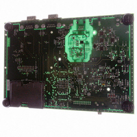
AT91RM3400-DK
Manufacturer Part Number
AT91RM3400-DK
Description
KIT DEV FOR AT91RM3400
Manufacturer
Atmel
Series
AT91SAM Smart ARMr
Type
MCUr
Datasheets
1.AT91RM3400-DK.pdf
(461 pages)
2.AT91RM3400-DK.pdf
(2 pages)
3.AT91RM3400-DK.pdf
(25 pages)
Specifications of AT91RM3400-DK
Contents
Evaluation Board, Software and Documentation
Processor To Be Evaluated
AT91RM3400
Data Bus Width
32 bit
Interface Type
RS-232, USB
For Use With/related Products
AT91RM3400
Lead Free Status / RoHS Status
Contains lead / RoHS non-compliant


Receiver and
Transmitter
Control
Synchronous and
Asynchronous
Modes
Transmitter
Operations
1790A–ATARM–11/03
Figure 93. Elementary Time Unit (ETU)
After reset, the receiver is disabled. The user must enable the receiver by setting the RXEN bit
in the Control Register (US_CR). However, the receiver registers can be programmed before
the receiver clock is enabled.
After reset, the transmitter is disabled. The user must enable it by setting the TXEN bit in the
Control Register (US_CR). However, the transmitter registers can be programmed before
being enabled.
The Receiver and the Transmitter can be enabled together or independently.
At any time, the software can perform a reset on the receiver or the transmitter of the USART
by setting the corresponding bit, RSTRX and RSTTX respectively, in the Control Register
(US_CR). The reset commands have the same effect as a hardware reset on the correspond-
ing logic. Regardless of what the receiver or the transmitter is performing, the communication
is immediately stopped.
The user can also independently disable the receiver or the transmitter by setting RXDIS and
TXDIS respectively in US_CR. If the receiver is disabled during a character reception, the
USART waits until the end of reception of the current character, then the reception is stopped.
If the transmitter is disabled while it is operating, the USART waits the end of transmission of
both the current character and character being stored in the Transmit Holding Register
(US_THR). If a time guard is programmed, it is handled normally.
The transmitter performs the same in both synchronous and asynchronous operating modes
(SYNC = 0 or SYNC = 1). One start bit, up to 9 data bits, one optional parity bit and up to two
stop bits are successively shifted out on the TXD pin at each falling edge of the programmed
serial clock.
The number of data bits is selected by the CHRL field and the MODE9 bit in the Mode Regis-
ter (US_MR). Nine bits are selected by setting the MODE 9 bit regardless of the CHRL field.
The parity bit is set according to the PAR field in US_MR. The even, odd, space, marked or
none parity bit can be configured. The MSBF field in US_MR configures which data bit is sent
first. If written at 1, the most significant bit is sent first. At 0, the less significant bit is sent first.
The number of stop bits is selected by the NBSTOP field in US_MR. The 1.5 stop bit is sup-
ported in asynchronous mode only.
ISO7816 I/O Line
ISO7816 Clock
on SCK
on TXD
ISO7816 Clock Cycles
FI_DI_RATIO
1 ETU
AT91RM3400
275
Related parts for AT91RM3400-DK
Image
Part Number
Description
Manufacturer
Datasheet
Request
R

Part Number:
Description:
DEV KIT FOR AVR/AVR32
Manufacturer:
Atmel
Datasheet:

Part Number:
Description:
INTERVAL AND WIPE/WASH WIPER CONTROL IC WITH DELAY
Manufacturer:
ATMEL Corporation
Datasheet:
Part Number:
Description:
Low-Voltage Voice-Switched IC for Hands-Free Operation
Manufacturer:
ATMEL Corporation
Datasheet:
Part Number:
Description:
MONOLITHIC INTEGRATED FEATUREPHONE CIRCUIT
Manufacturer:
ATMEL Corporation
Datasheet:
Part Number:
Description:
AM-FM Receiver IC U4255BM-M
Manufacturer:
ATMEL Corporation
Datasheet:
Part Number:
Description:
Monolithic Integrated Feature Phone Circuit
Manufacturer:
ATMEL Corporation
Datasheet:
Part Number:
Description:
Multistandard Video-IF and Quasi Parallel Sound Processing
Manufacturer:
ATMEL Corporation
Datasheet:
Part Number:
Description:
High-performance EE PLD
Manufacturer:
ATMEL Corporation
Datasheet:
Part Number:
Description:
8-bit Flash Microcontroller
Manufacturer:
ATMEL Corporation
Datasheet:
Part Number:
Description:
2-Wire Serial EEPROM
Manufacturer:
ATMEL Corporation
Datasheet: