AT91RM3400-DK Atmel, AT91RM3400-DK Datasheet - Page 454
AT91RM3400-DK
Manufacturer Part Number
AT91RM3400-DK
Description
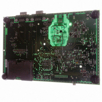
KIT DEV FOR AT91RM3400
Manufacturer
Atmel
Series
AT91SAM Smart ARMr
Type
MCUr
Datasheets
1.AT91RM3400-DK.pdf
(461 pages)
2.AT91RM3400-DK.pdf
(2 pages)
3.AT91RM3400-DK.pdf
(25 pages)
Specifications of AT91RM3400-DK
Contents
Evaluation Board, Software and Documentation
Processor To Be Evaluated
AT91RM3400
Data Bus Width
32 bit
Interface Type
RS-232, USB
For Use With/related Products
AT91RM3400
Lead Free Status / RoHS Status
Contains lead / RoHS non-compliant


1790A–ATARM–11/03
Parallel Input/Output Controller (PIO) ....................................................... 203
UART Operations............................................................................................ 183
Debug Unit User Interface ............................................................................. 190
Overview.......................................................................................................... 203
Block Diagram................................................................................................. 204
Product Dependencies................................................................................... 205
Functional Description................................................................................... 206
I/O Lines Programming Example .................................................................. 211
Parallel Input/Output Controller (PIO) User Interface.................................. 212
Baud Rate Generator ................................................................................... 183
Receiver ....................................................................................................... 184
Transmitter ................................................................................................... 186
Peripheral Data Controller............................................................................ 187
Test Modes .................................................................................................. 187
Debug Communication Channel Support..................................................... 189
Chip Identifier ............................................................................................... 189
ICE Access Prevention ................................................................................ 189
Debug Unit Control Register ........................................................................ 191
Debug Unit Mode Register ........................................................................... 192
Debug Unit Interrupt Enable Register .......................................................... 193
Debug Unit Interrupt Disable Register ......................................................... 194
Debug Unit Interrupt Mask Register ............................................................. 195
Debug Unit Status Register.......................................................................... 196
Debug Unit Receiver Holding Register ........................................................ 198
Debug Unit Baud Rate Generator Register.................................................. 199
Debug Unit Chip ID Register ........................................................................ 200
Debug Unit Chip ID Extension Register ....................................................... 202
Debug Unit Force NTRST Register.............................................................. 202
Pin Multiplexing ............................................................................................ 205
External Interrupt Lines ................................................................................ 205
Power Management ..................................................................................... 205
Interrupt Generation ..................................................................................... 205
Pull-up Resistor Control ............................................................................... 207
I/O Line or Peripheral Function Selection .................................................... 207
Peripheral A or B Selection .......................................................................... 207
Output Control.............................................................................................. 207
Synchronous Data Output............................................................................ 208
Multi Drive Control (Open Drain) .................................................................. 208
Output Line Timings ..................................................................................... 208
Inputs ........................................................................................................... 209
Input Glitch Filtering ..................................................................................... 209
Input Change Interrupt ................................................................................. 210
PIO Enable Register .................................................................................... 214
PIO Disable Register.................................................................................... 214
PIO Status Register ..................................................................................... 215
AT91RM3400
vii
Related parts for AT91RM3400-DK
Image
Part Number
Description
Manufacturer
Datasheet
Request
R

Part Number:
Description:
DEV KIT FOR AVR/AVR32
Manufacturer:
Atmel
Datasheet:

Part Number:
Description:
INTERVAL AND WIPE/WASH WIPER CONTROL IC WITH DELAY
Manufacturer:
ATMEL Corporation
Datasheet:
Part Number:
Description:
Low-Voltage Voice-Switched IC for Hands-Free Operation
Manufacturer:
ATMEL Corporation
Datasheet:
Part Number:
Description:
MONOLITHIC INTEGRATED FEATUREPHONE CIRCUIT
Manufacturer:
ATMEL Corporation
Datasheet:
Part Number:
Description:
AM-FM Receiver IC U4255BM-M
Manufacturer:
ATMEL Corporation
Datasheet:
Part Number:
Description:
Monolithic Integrated Feature Phone Circuit
Manufacturer:
ATMEL Corporation
Datasheet:
Part Number:
Description:
Multistandard Video-IF and Quasi Parallel Sound Processing
Manufacturer:
ATMEL Corporation
Datasheet:
Part Number:
Description:
High-performance EE PLD
Manufacturer:
ATMEL Corporation
Datasheet:
Part Number:
Description:
8-bit Flash Microcontroller
Manufacturer:
ATMEL Corporation
Datasheet:
Part Number:
Description:
2-Wire Serial EEPROM
Manufacturer:
ATMEL Corporation
Datasheet: