AT91RM3400-DK Atmel, AT91RM3400-DK Datasheet - Page 249
AT91RM3400-DK
Manufacturer Part Number
AT91RM3400-DK
Description
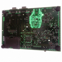
KIT DEV FOR AT91RM3400
Manufacturer
Atmel
Series
AT91SAM Smart ARMr
Type
MCUr
Datasheets
1.AT91RM3400-DK.pdf
(461 pages)
2.AT91RM3400-DK.pdf
(2 pages)
3.AT91RM3400-DK.pdf
(25 pages)
Specifications of AT91RM3400-DK
Contents
Evaluation Board, Software and Documentation
Processor To Be Evaluated
AT91RM3400
Data Bus Width
32 bit
Interface Type
RS-232, USB
For Use With/related Products
AT91RM3400
Lead Free Status / RoHS Status
Contains lead / RoHS non-compliant


SPI Chip Select Register
Name:
Access Type:
• CPOL: Clock Polarity
0 = The inactive state value of SPCK is logic level zero.
1 = The inactive state value of SPCK is logic level one.
CPOL is used to determine the inactive state value of the serial clock (SPCK). It is used with NCPHA to produce the
required clock/data relationship between master and slave devices.
• NCPHA: Clock Phase
0 = Data is changed on the leading edge of SPCK and captured on the following edge of SPCK.
1 = Data is captured on the leading edge of SPCK and changed on the following edge of SPCK.
NCPHA determines which edge of SPCK causes data to change and which edge causes data to be captured. NCPHA is
used with CPOL to produce the required clock/data relationship between master and slave devices.
• BITS: Bits Per Transfer
The BITS field determines the number of data bits transferred. Reserved values should not be used.
1790A–ATARM–11/03
31
23
15
7
SPI_CSR0... SPI_CSR3
Read/write
30
22
14
6
BITS[3:0]
0000
0001
0010
0011
0100
0101
0110
0111
1000
1001
1010
1011
1100
1101
1110
1111
BITS
29
21
13
5
28
20
12
4
DLYBCT
DLYBS
SCBR
27
19
11
–
3
Bits Per Transfer
26
18
10
2
–
Reserved
Reserved
Reserved
Reserved
Reserved
Reserved
Reserved
10
11
12
13
14
15
16
8
9
NCPHA
AT91RM3400
25
17
9
1
CPOL
24
16
8
0
249
Related parts for AT91RM3400-DK
Image
Part Number
Description
Manufacturer
Datasheet
Request
R

Part Number:
Description:
DEV KIT FOR AVR/AVR32
Manufacturer:
Atmel
Datasheet:

Part Number:
Description:
INTERVAL AND WIPE/WASH WIPER CONTROL IC WITH DELAY
Manufacturer:
ATMEL Corporation
Datasheet:
Part Number:
Description:
Low-Voltage Voice-Switched IC for Hands-Free Operation
Manufacturer:
ATMEL Corporation
Datasheet:
Part Number:
Description:
MONOLITHIC INTEGRATED FEATUREPHONE CIRCUIT
Manufacturer:
ATMEL Corporation
Datasheet:
Part Number:
Description:
AM-FM Receiver IC U4255BM-M
Manufacturer:
ATMEL Corporation
Datasheet:
Part Number:
Description:
Monolithic Integrated Feature Phone Circuit
Manufacturer:
ATMEL Corporation
Datasheet:
Part Number:
Description:
Multistandard Video-IF and Quasi Parallel Sound Processing
Manufacturer:
ATMEL Corporation
Datasheet:
Part Number:
Description:
High-performance EE PLD
Manufacturer:
ATMEL Corporation
Datasheet:
Part Number:
Description:
8-bit Flash Microcontroller
Manufacturer:
ATMEL Corporation
Datasheet:
Part Number:
Description:
2-Wire Serial EEPROM
Manufacturer:
ATMEL Corporation
Datasheet: