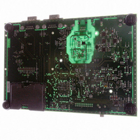
AT91RM3400-DK Atmel, AT91RM3400-DK Datasheet - Page 396

AT91RM3400-DK
Manufacturer Part Number
AT91RM3400-DK
Description
KIT DEV FOR AT91RM3400
Manufacturer
Atmel
Series
AT91SAM Smart ARMr
Type
MCUr
Datasheets
1.AT91RM3400-DK.pdf
(461 pages)
2.AT91RM3400-DK.pdf
(2 pages)
3.AT91RM3400-DK.pdf
(25 pages)
Specifications of AT91RM3400-DK
Contents
Evaluation Board, Software and Documentation
Processor To Be Evaluated
AT91RM3400
Data Bus Width
32 bit
Interface Type
RS-232, USB
For Use With/related Products
AT91RM3400
Lead Free Status / RoHS Status
Contains lead / RoHS non-compliant
- Current page: 396 of 461
- Download datasheet (6Mb)
Block Diagram
Figure 161. USB Device Port Block Diagram
396
MCK
UDPCK
udp_int
External Resume
Atmel Bridge
AT91RM3400
MCU
APB
Bus
to
Access to the UDP is via the APB bus interface. Read and write to the data FIFO are done by
reading and writing 8-bit values to APB registers.
The UDP peripheral requires two clocks: one peripheral clock used by the MCK domain and a
48 MHz clock used by the 12 MHz domain.
A USB 2.0 full-speed pad is embedded and controlled by the SIE.
The signal external_resume is optional. It allows the UDP peripheral to wake-up once in sys-
tem mode. The host will then be notified that the device asks for a resume. This optional
feature must be also negotiated with the host during the enumeration.
U
s
e
n
e
a
c
e
r
r
I
t
f
W
a
p
p
e
Master Clock
Domain
r
r
USB Device
FIFO
RAM
Dual
Port
Recovered 12 MHz
Domain
W
a
p
p
e
r
r
Suspend/Resume Logic
12 MHz
Interface
Engine
Serial
SIE
txoen
eopn
txd
rxdm
rxd
rxdp
Transceiver
Embedded
1790A–ATARM–11/03
USB
DM
DP
Related parts for AT91RM3400-DK
Image
Part Number
Description
Manufacturer
Datasheet
Request
R

Part Number:
Description:
DEV KIT FOR AVR/AVR32
Manufacturer:
Atmel
Datasheet:

Part Number:
Description:
INTERVAL AND WIPE/WASH WIPER CONTROL IC WITH DELAY
Manufacturer:
ATMEL Corporation
Datasheet:

Part Number:
Description:
Low-Voltage Voice-Switched IC for Hands-Free Operation
Manufacturer:
ATMEL Corporation
Datasheet:

Part Number:
Description:
MONOLITHIC INTEGRATED FEATUREPHONE CIRCUIT
Manufacturer:
ATMEL Corporation
Datasheet:

Part Number:
Description:
AM-FM Receiver IC U4255BM-M
Manufacturer:
ATMEL Corporation
Datasheet:

Part Number:
Description:
Monolithic Integrated Feature Phone Circuit
Manufacturer:
ATMEL Corporation
Datasheet:

Part Number:
Description:
Multistandard Video-IF and Quasi Parallel Sound Processing
Manufacturer:
ATMEL Corporation
Datasheet:

Part Number:
Description:
High-performance EE PLD
Manufacturer:
ATMEL Corporation
Datasheet:

Part Number:
Description:
8-bit Flash Microcontroller
Manufacturer:
ATMEL Corporation
Datasheet:

Part Number:
Description:
2-Wire Serial EEPROM
Manufacturer:
ATMEL Corporation
Datasheet:


