C8051F020DK Silicon Laboratories Inc, C8051F020DK Datasheet - Page 168
C8051F020DK
Manufacturer Part Number
C8051F020DK
Description
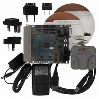
DEV KIT FOR F020/F021/F022/F023
Manufacturer
Silicon Laboratories Inc
Type
MCUr
Datasheet
1.C8051F020DK.pdf
(272 pages)
Specifications of C8051F020DK
Contents
Evaluation Board, Power Supply, USB Cables, Adapter and Documentation
Processor To Be Evaluated
C8051F02x
Interface Type
USB
Silicon Manufacturer
Silicon Labs
Core Architecture
8051
Silicon Core Number
C8051F020
Silicon Family Name
C8051F02x
Lead Free Status / RoHS Status
Contains lead / RoHS non-compliant
For Use With/related Products
Silicon Laboratories C8051 F020/021/022/023
Lead Free Status / Rohs Status
Lead free / RoHS Compliant
Other names
336-1200
Available stocks
Company
Part Number
Manufacturer
Quantity
Price
Company:

Part Number:
C8051F020DK
Manufacturer:
SiliconL
Quantity:
10


C8051F020/1/2/3
17.1.8. Crossbar Pin Assignment Example
In this example (Figure 17.6), we configure the Crossbar to allocate Port pins for UART0, the SMBus, UART1,
/INT0, and /INT1 (8 pins total). Additionally, we configure the External Memory Interface to operate in Multiplexed
mode and to appear on the Low ports. Further, we configure P1.2, P1.3, and P1.4 for Analog Input mode so that the
voltages at these pins can be measured by ADC1. The configuration steps are as follows:
168
1.
2.
3.
4.
5.
6.
7.
XBR0, XBR1, and XBR2 are set such that UART0EN = 1, SMB0EN = 1, INT0E = 1, INT1E
= 1, and EMIFLE = 1. Thus: XBR0 = 0x05, XBR1 = 0x14, and XBR2 = 0x02.
We configure the External Memory Interface to use Multiplexed mode and to appear on the
Low ports. PRTSEL = 0, EMD2 = 0.
We configure the desired Port 1 pins to Analog Input mode by setting P1MDIN to 0xE3 (P1.4,
P1.3, and P1.2 are Analog Inputs, so their associated P1MDIN bits are set to logic 0).
We enable the Crossbar by setting XBARE = 1: XBR2 = 0x46.
-
-
-
-
-
-
-
We set the UART0 TX pin (TX0, P0.0), UART1 TX pin (TX1, P0.4), ALE, /RD, /WR
(P0.[7:3]) outputs to Push-Pull by setting P0MDOUT = 0xF1.
We configure the output modes of the EMIF Ports (P2, P3) to Push-Pull by setting P2MDOUT
= 0xFF and P3MDOUT = 0xFF.
We explicitly disable the output drivers on the 3 Analog Input pins by setting P1MDOUT =
0x00 (configure outputs to Open-Drain) and P1 = 0xFF (a logic 1 selects the high-impedance
state).
UART0 has the highest priority, so P0.0 is assigned to TX0, and P0.1 is assigned to RX0.
The SMBus is next in priority order, so P0.2 is assigned to SDA, and P0.3 is assigned to SCL.
UART1 is next in priority order, so P0.4 is assigned to TX1. Because the External Memory Inter-
face is selected on the lower Ports, EMIFLE = 1, which causes the Crossbar to skip P0.6 (/RD) and
P0.7 (/WR). Because the External Memory Interface is configured in Multiplexed mode, the Cross-
bar will also skip P0.5 (ALE). RX1 is assigned to the next non-skipped pin, which in this case is
P1.0.
/INT0 is next in priority order, so it is assigned to P1.1.
P1MDIN is set to 0xE3, which configures P1.2, P1.3, and P1.4 as Analog Inputs, causing the
Crossbar to skip these pins.
/INT1 is next in priority order, so it is assigned to the next non-skipped pin, which is P1.5.
The External Memory Interface will drive Ports 2 and 3 (denoted by red dots in Figure 17.6) during
the execution of an off-chip MOVX instruction.
Rev. 1.4
Related parts for C8051F020DK
Image
Part Number
Description
Manufacturer
Datasheet
Request
R

Part Number:
Description:
SMD/C°/SINGLE-ENDED OUTPUT SILICON OSCILLATOR
Manufacturer:
Silicon Laboratories Inc
Part Number:
Description:
Manufacturer:
Silicon Laboratories Inc
Datasheet:
Part Number:
Description:
N/A N/A/SI4010 AES KEYFOB DEMO WITH LCD RX
Manufacturer:
Silicon Laboratories Inc
Datasheet:
Part Number:
Description:
N/A N/A/SI4010 SIMPLIFIED KEY FOB DEMO WITH LED RX
Manufacturer:
Silicon Laboratories Inc
Datasheet:
Part Number:
Description:
N/A/-40 TO 85 OC/EZLINK MODULE; F930/4432 HIGH BAND (REV E/B1)
Manufacturer:
Silicon Laboratories Inc
Part Number:
Description:
EZLink Module; F930/4432 Low Band (rev e/B1)
Manufacturer:
Silicon Laboratories Inc
Part Number:
Description:
I°/4460 10 DBM RADIO TEST CARD 434 MHZ
Manufacturer:
Silicon Laboratories Inc
Part Number:
Description:
I°/4461 14 DBM RADIO TEST CARD 868 MHZ
Manufacturer:
Silicon Laboratories Inc
Part Number:
Description:
I°/4463 20 DBM RFSWITCH RADIO TEST CARD 460 MHZ
Manufacturer:
Silicon Laboratories Inc
Part Number:
Description:
I°/4463 20 DBM RADIO TEST CARD 868 MHZ
Manufacturer:
Silicon Laboratories Inc
Part Number:
Description:
I°/4463 27 DBM RADIO TEST CARD 868 MHZ
Manufacturer:
Silicon Laboratories Inc
Part Number:
Description:
I°/4463 SKYWORKS 30 DBM RADIO TEST CARD 915 MHZ
Manufacturer:
Silicon Laboratories Inc
Part Number:
Description:
N/A N/A/-40 TO 85 OC/4463 RFMD 30 DBM RADIO TEST CARD 915 MHZ
Manufacturer:
Silicon Laboratories Inc
Part Number:
Description:
I°/4463 20 DBM RADIO TEST CARD 169 MHZ
Manufacturer:
Silicon Laboratories Inc