C8051F020DK Silicon Laboratories Inc, C8051F020DK Datasheet - Page 28
C8051F020DK
Manufacturer Part Number
C8051F020DK
Description
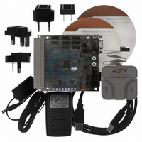
DEV KIT FOR F020/F021/F022/F023
Manufacturer
Silicon Laboratories Inc
Type
MCUr
Datasheet
1.C8051F020DK.pdf
(272 pages)
Specifications of C8051F020DK
Contents
Evaluation Board, Power Supply, USB Cables, Adapter and Documentation
Processor To Be Evaluated
C8051F02x
Interface Type
USB
Silicon Manufacturer
Silicon Labs
Core Architecture
8051
Silicon Core Number
C8051F020
Silicon Family Name
C8051F02x
Lead Free Status / RoHS Status
Contains lead / RoHS non-compliant
For Use With/related Products
Silicon Laboratories C8051 F020/021/022/023
Lead Free Status / Rohs Status
Lead free / RoHS Compliant
Other names
336-1200
Available stocks
Company
Part Number
Manufacturer
Quantity
Price
Company:

Part Number:
C8051F020DK
Manufacturer:
SiliconL
Quantity:
10


C8051F020/1/2/3
1.7.
The C8051F020/1 has an on-chip 12-bit SAR ADC (ADC0) with a 9-channel input multiplexer and programmable
gain amplifier. With a maximum throughput of 100 ksps, the ADC offers true 12-bit accuracy with an INL of ±1LSB.
C8051F022/3 devices include a 10-bit SAR ADC with similar specifications and configuration options. The ADC0
voltage reference is selected between the DAC0 output and an external VREF pin. On C8051F020/2 devices, ADC0
has its own dedicated VREF0 input pin; on C8051F021/3 devices, the ADC0 shares the VREFA input pin with the 8-
bit ADC1. The on-chip 15 ppm/°C voltage reference may generate the voltage reference for other system components
or the on-chip ADCs via the VREF output pin.
The ADC is under full control of the CIP-51 microcontroller via its associated Special Function Registers. One input
channel is tied to an internal temperature sensor, while the other eight channels are available externally. Each pair of
the eight external input channels can be configured as either two single-ended inputs or a single differential input.
The system controller can also put the ADC into shutdown mode to save power.
A programmable gain amplifier follows the analog multiplexer. The gain can be set in software from 0.5 to 16 in
powers of 2. The gain stage can be especially useful when different ADC input channels have widely varied input
voltage signals, or when it is necessary to "zoom in" on a signal with a large DC offset (in differential mode, a DAC
could be used to provide the DC offset).
Conversions can be started in four ways; a software command, an overflow of Timer 2, an overflow of Timer 3, or an
external signal input. This flexibility allows the start of conversion to be triggered by software events, external HW
signals, or a periodic timer overflow signal. Conversion completions are indicated by a status bit and an interrupt (if
enabled). The resulting 10 or 12-bit data word is latched into two SFRs upon completion of a conversion. The data
can be right or left justified in these registers under software control.
Window Compare registers for the ADC data can be configured to interrupt the controller when ADC data is within
or outside of a specified range. The ADC can monitor a key voltage continuously in background mode, but not inter-
rupt the controller unless the converted data is within the specified window.
28
AIN0.0
AIN0.1
AIN0.2
AIN0.3
AIN0.4
AIN0.5
AIN0.6
AIN0.7
12-Bit Analog to Digital Converter
Analog Multiplexer
AGND
SENSOR
TEMP
+
+
+
+
-
-
-
-
AMUX
(SE or
9-to-1
DIFF)
Figure 1.11. 12-Bit ADC Block Diagram
Programmable Gain
X
Amplifier
Configuration, Control, and Data
External VREF
+
-
DAC0 Output
AV+
Rev. 1.4
Registers
Pin
ADC
VREF
12-Bit
SAR
Start
Conversion
Window Compare
12
Logic
Write to AD0BUSY
Timer 3 Overflow
CNVSTR
Timer 2 Overflow
ADC Data
Registers
Conversion
Complete
Compare
Interrupt
Interrupt
Window
Related parts for C8051F020DK
Image
Part Number
Description
Manufacturer
Datasheet
Request
R

Part Number:
Description:
SMD/C°/SINGLE-ENDED OUTPUT SILICON OSCILLATOR
Manufacturer:
Silicon Laboratories Inc
Part Number:
Description:
Manufacturer:
Silicon Laboratories Inc
Datasheet:
Part Number:
Description:
N/A N/A/SI4010 AES KEYFOB DEMO WITH LCD RX
Manufacturer:
Silicon Laboratories Inc
Datasheet:
Part Number:
Description:
N/A N/A/SI4010 SIMPLIFIED KEY FOB DEMO WITH LED RX
Manufacturer:
Silicon Laboratories Inc
Datasheet:
Part Number:
Description:
N/A/-40 TO 85 OC/EZLINK MODULE; F930/4432 HIGH BAND (REV E/B1)
Manufacturer:
Silicon Laboratories Inc
Part Number:
Description:
EZLink Module; F930/4432 Low Band (rev e/B1)
Manufacturer:
Silicon Laboratories Inc
Part Number:
Description:
I°/4460 10 DBM RADIO TEST CARD 434 MHZ
Manufacturer:
Silicon Laboratories Inc
Part Number:
Description:
I°/4461 14 DBM RADIO TEST CARD 868 MHZ
Manufacturer:
Silicon Laboratories Inc
Part Number:
Description:
I°/4463 20 DBM RFSWITCH RADIO TEST CARD 460 MHZ
Manufacturer:
Silicon Laboratories Inc
Part Number:
Description:
I°/4463 20 DBM RADIO TEST CARD 868 MHZ
Manufacturer:
Silicon Laboratories Inc
Part Number:
Description:
I°/4463 27 DBM RADIO TEST CARD 868 MHZ
Manufacturer:
Silicon Laboratories Inc
Part Number:
Description:
I°/4463 SKYWORKS 30 DBM RADIO TEST CARD 915 MHZ
Manufacturer:
Silicon Laboratories Inc
Part Number:
Description:
N/A N/A/-40 TO 85 OC/4463 RFMD 30 DBM RADIO TEST CARD 915 MHZ
Manufacturer:
Silicon Laboratories Inc
Part Number:
Description:
I°/4463 20 DBM RADIO TEST CARD 169 MHZ
Manufacturer:
Silicon Laboratories Inc