C8051F020DK Silicon Laboratories Inc, C8051F020DK Datasheet - Page 185
C8051F020DK
Manufacturer Part Number
C8051F020DK
Description
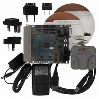
DEV KIT FOR F020/F021/F022/F023
Manufacturer
Silicon Laboratories Inc
Type
MCUr
Datasheet
1.C8051F020DK.pdf
(272 pages)
Specifications of C8051F020DK
Contents
Evaluation Board, Power Supply, USB Cables, Adapter and Documentation
Processor To Be Evaluated
C8051F02x
Interface Type
USB
Silicon Manufacturer
Silicon Labs
Core Architecture
8051
Silicon Core Number
C8051F020
Silicon Family Name
C8051F02x
Lead Free Status / RoHS Status
Contains lead / RoHS non-compliant
For Use With/related Products
Silicon Laboratories C8051 F020/021/022/023
Lead Free Status / Rohs Status
Lead free / RoHS Compliant
Other names
336-1200
Available stocks
Company
Part Number
Manufacturer
Quantity
Price
Company:

Part Number:
C8051F020DK
Manufacturer:
SiliconL
Quantity:
10


C8051F020/1/2/3
18.2. SMBus Protocol
Two types of data transfers are possible: data transfers from a master transmitter to an addressed slave receiver
(WRITE), and data transfers from an addressed slave transmitter to a master receiver (READ). The master device ini-
tiates both types of data transfers and provides the serial clock pulses on SCL. Note: multiple master devices on the
same bus are supported. If two or more masters attempt to initiate a data transfer simultaneously, an arbitration
scheme is employed with a single master always winning the arbitration. Note that it is not necessary to specify one
device as the master in a system; any device who transmits a START and a slave address becomes the master for that
transfer.
A typical SMBus transaction consists of a START condition followed by an address byte (Bits7-1: 7-bit slave
address; Bit0: R/W direction bit), one or more bytes of data, and a STOP condition. Each byte that is received (by a
master or slave) must be acknowledged (ACK) with a low SDA during a high SCL (see Figure 18.3). If the receiving
device does not ACK, the transmitting device will read a “not acknowledge” (NACK), which is a high SDA during a
high SCL.
The direction bit (R/W) occupies the least-significant bit position of the address. The direction bit is set to logic 1 to
indicate a "READ" operation and cleared to logic 0 to indicate a "WRITE" operation.
All transactions are initiated by a master, with one or more addressed slave devices as the target. The master gener-
ates the START condition and then transmits the slave address and direction bit. If the transaction is a WRITE opera-
tion from the master to the slave, the master transmits the data a byte at a time waiting for an ACK from the slave at
the end of each byte. For READ operations, the slave transmits the data waiting for an ACK from the master at the
end of each byte. At the end of the data transfer, the master generates a STOP condition to terminate the transaction
and free the bus. Figure 18.3 illustrates a typical SMBus transaction.
Figure 18.3. SMBus Transaction
SCL
SDA
SLA6
SLA5-0
R/W
D7
D6-0
START
Slave Address + R/W
ACK
Data Byte
NACK
STOP
18.2.1. Arbitration
A master may start a transfer only if the bus is free. The bus is free after a STOP condition or after the SCL and SDA
lines remain high for a specified time (see
Section
18.2.4). In the event that two or more devices attempt to begin a
transfer at the same time, an arbitration scheme is employed to force one master to give up the bus. The master
devices continue transmitting until one attempts a HIGH while the other transmits a LOW. Since the bus is open-
drain, the bus will be pulled LOW. The master attempting the HIGH will detect a LOW SDA and give up the bus. The
winning master continues its transmission without interruption; the losing master becomes a slave and receives the
rest of the transfer. This arbitration scheme is non-destructive: one device always wins, and no data is lost.
18.2.2. Clock Low Extension
2
SMBus provides a clock synchronization mechanism, similar to I
C, which allows devices with different speed capa-
bilities to coexist on the bus. A clock-low extension is used during a transfer in order to allow slower slave devices to
communicate with faster masters. The slave may temporarily hold the SCL line LOW to extend the clock low period,
effectively decreasing the serial clock frequency.
Rev. 1.4
185
Related parts for C8051F020DK
Image
Part Number
Description
Manufacturer
Datasheet
Request
R

Part Number:
Description:
SMD/C°/SINGLE-ENDED OUTPUT SILICON OSCILLATOR
Manufacturer:
Silicon Laboratories Inc
Part Number:
Description:
Manufacturer:
Silicon Laboratories Inc
Datasheet:
Part Number:
Description:
N/A N/A/SI4010 AES KEYFOB DEMO WITH LCD RX
Manufacturer:
Silicon Laboratories Inc
Datasheet:
Part Number:
Description:
N/A N/A/SI4010 SIMPLIFIED KEY FOB DEMO WITH LED RX
Manufacturer:
Silicon Laboratories Inc
Datasheet:
Part Number:
Description:
N/A/-40 TO 85 OC/EZLINK MODULE; F930/4432 HIGH BAND (REV E/B1)
Manufacturer:
Silicon Laboratories Inc
Part Number:
Description:
EZLink Module; F930/4432 Low Band (rev e/B1)
Manufacturer:
Silicon Laboratories Inc
Part Number:
Description:
I°/4460 10 DBM RADIO TEST CARD 434 MHZ
Manufacturer:
Silicon Laboratories Inc
Part Number:
Description:
I°/4461 14 DBM RADIO TEST CARD 868 MHZ
Manufacturer:
Silicon Laboratories Inc
Part Number:
Description:
I°/4463 20 DBM RFSWITCH RADIO TEST CARD 460 MHZ
Manufacturer:
Silicon Laboratories Inc
Part Number:
Description:
I°/4463 20 DBM RADIO TEST CARD 868 MHZ
Manufacturer:
Silicon Laboratories Inc
Part Number:
Description:
I°/4463 27 DBM RADIO TEST CARD 868 MHZ
Manufacturer:
Silicon Laboratories Inc
Part Number:
Description:
I°/4463 SKYWORKS 30 DBM RADIO TEST CARD 915 MHZ
Manufacturer:
Silicon Laboratories Inc
Part Number:
Description:
N/A N/A/-40 TO 85 OC/4463 RFMD 30 DBM RADIO TEST CARD 915 MHZ
Manufacturer:
Silicon Laboratories Inc
Part Number:
Description:
I°/4463 20 DBM RADIO TEST CARD 169 MHZ
Manufacturer:
Silicon Laboratories Inc