C8051F020DK Silicon Laboratories Inc, C8051F020DK Datasheet - Page 181
C8051F020DK
Manufacturer Part Number
C8051F020DK
Description
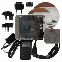
DEV KIT FOR F020/F021/F022/F023
Manufacturer
Silicon Laboratories Inc
Type
MCUr
Datasheet
1.C8051F020DK.pdf
(272 pages)
Specifications of C8051F020DK
Contents
Evaluation Board, Power Supply, USB Cables, Adapter and Documentation
Processor To Be Evaluated
C8051F02x
Interface Type
USB
Silicon Manufacturer
Silicon Labs
Core Architecture
8051
Silicon Core Number
C8051F020
Silicon Family Name
C8051F02x
Lead Free Status / RoHS Status
Contains lead / RoHS non-compliant
For Use With/related Products
Silicon Laboratories C8051 F020/021/022/023
Lead Free Status / Rohs Status
Lead free / RoHS Compliant
Other names
336-1200
Available stocks
Company
Part Number
Manufacturer
Quantity
Price
Company:

Part Number:
C8051F020DK
Manufacturer:
SiliconL
Quantity:
10


Bits7-0:
Note:
Bits7-0:
Note:
P6.7
P7.7
R/W
R/W
Bit7
Bit7
P6.[7:0]: Port6 Output Latch Bits.
Write - Output appears on I/O pins.
0: Logic Low Output.
1: Logic High Output (Open-Drain if corresponding P74OUT bit = 0). See Figure 17.20.
Read - Returns states of I/O pins.
0: P6.n pin is logic low.
1: P6.n pin is logic high.
P6.[7:0] can be driven by the External Data Memory Interface (as Address[15:8] in Multiplexed
mode, or as Address[7:0] in Non-multiplexed mode). See
ORY INTERFACE AND ON-CHIP XRAM” on page 145
Memory Interface.
P7.[7:0]: Port7 Output Latch Bits.
Write - Output appears on I/O pins.
0: Logic Low Output.
1: Logic High Output (Open-Drain if corresponding P74OUT bit = 0). See Figure 17.20.
Read - Returns states of I/O pins.
0: P7.n pin is logic low.
1: P7.n pin is logic high.
P7.[7:0] can be driven by the External Data Memory Interface (as AD[7:0] in Multiplexed mode, or
as D[7:0] in Non-multiplexed mode). See
FACE AND ON-CHIP XRAM” on page 145
Interface.
P6.6
P7.6
R/W
R/W
Bit6
Bit6
P6.5
P7.5
R/W
R/W
Bit5
Bit5
Figure 17.23. P6: Port6 Data Register
Figure 17.24. P7: Port7 Data Register
P6.4
P7.4
R/W
R/W
Bit4
Bit4
P6.3
P7.3
Section “16. EXTERNAL DATA MEMORY INTER-
R/W
R/W
Bit3
Bit3
Rev. 1.4
for more information about the External Memory
P6.2
P7.2
R/W
R/W
Bit2
Bit2
Section “16. EXTERNAL DATA MEM-
for more information about the External
P6.1
P7.1
C8051F020/1/2/3
R/W
R/W
Bit1
Bit1
P6.0
P7.0
R/W
R/W
Bit0
Bit0
SFR Address:
SFR Address:
Reset Value
11111111
Reset Value
11111111
0x86
0x96
181
Related parts for C8051F020DK
Image
Part Number
Description
Manufacturer
Datasheet
Request
R

Part Number:
Description:
SMD/C°/SINGLE-ENDED OUTPUT SILICON OSCILLATOR
Manufacturer:
Silicon Laboratories Inc
Part Number:
Description:
Manufacturer:
Silicon Laboratories Inc
Datasheet:
Part Number:
Description:
N/A N/A/SI4010 AES KEYFOB DEMO WITH LCD RX
Manufacturer:
Silicon Laboratories Inc
Datasheet:
Part Number:
Description:
N/A N/A/SI4010 SIMPLIFIED KEY FOB DEMO WITH LED RX
Manufacturer:
Silicon Laboratories Inc
Datasheet:
Part Number:
Description:
N/A/-40 TO 85 OC/EZLINK MODULE; F930/4432 HIGH BAND (REV E/B1)
Manufacturer:
Silicon Laboratories Inc
Part Number:
Description:
EZLink Module; F930/4432 Low Band (rev e/B1)
Manufacturer:
Silicon Laboratories Inc
Part Number:
Description:
I°/4460 10 DBM RADIO TEST CARD 434 MHZ
Manufacturer:
Silicon Laboratories Inc
Part Number:
Description:
I°/4461 14 DBM RADIO TEST CARD 868 MHZ
Manufacturer:
Silicon Laboratories Inc
Part Number:
Description:
I°/4463 20 DBM RFSWITCH RADIO TEST CARD 460 MHZ
Manufacturer:
Silicon Laboratories Inc
Part Number:
Description:
I°/4463 20 DBM RADIO TEST CARD 868 MHZ
Manufacturer:
Silicon Laboratories Inc
Part Number:
Description:
I°/4463 27 DBM RADIO TEST CARD 868 MHZ
Manufacturer:
Silicon Laboratories Inc
Part Number:
Description:
I°/4463 SKYWORKS 30 DBM RADIO TEST CARD 915 MHZ
Manufacturer:
Silicon Laboratories Inc
Part Number:
Description:
N/A N/A/-40 TO 85 OC/4463 RFMD 30 DBM RADIO TEST CARD 915 MHZ
Manufacturer:
Silicon Laboratories Inc
Part Number:
Description:
I°/4463 20 DBM RADIO TEST CARD 169 MHZ
Manufacturer:
Silicon Laboratories Inc