C8051F020DK Silicon Laboratories Inc, C8051F020DK Datasheet - Page 193
C8051F020DK
Manufacturer Part Number
C8051F020DK
Description
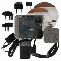
DEV KIT FOR F020/F021/F022/F023
Manufacturer
Silicon Laboratories Inc
Type
MCUr
Datasheet
1.C8051F020DK.pdf
(272 pages)
Specifications of C8051F020DK
Contents
Evaluation Board, Power Supply, USB Cables, Adapter and Documentation
Processor To Be Evaluated
C8051F02x
Interface Type
USB
Silicon Manufacturer
Silicon Labs
Core Architecture
8051
Silicon Core Number
C8051F020
Silicon Family Name
C8051F02x
Lead Free Status / RoHS Status
Contains lead / RoHS non-compliant
For Use With/related Products
Silicon Laboratories C8051 F020/021/022/023
Lead Free Status / Rohs Status
Lead free / RoHS Compliant
Other names
336-1200
Available stocks
Company
Part Number
Manufacturer
Quantity
Price
Company:

Part Number:
C8051F020DK
Manufacturer:
SiliconL
Quantity:
10


18.4.3. Data Register
The SMBus0 Data register SMB0DAT holds a byte of serial data to be transmitted or one that has just been received.
Software can read or write to this register while the SI flag is set to logic 1; software should not attempt to access the
SMB0DAT register when the SMBus is enabled and the SI flag is cleared to logic 0 since the hardware may be in the
process of shifting a byte of data in or out of the register.
Data in SMB0DAT is always shifted out MSB first. After a byte has been received, the first bit of received data is
located at the MSB of SMB0DAT. While data is being shifted out, data on the bus is simultaneously being shifted in.
Therefore, SMB0DAT always contains the last data byte present on the bus. In the event of lost arbitration, the transi-
tion from master transmitter to slave receiver is made with the correct data in SMB0DAT.
18.4.4. Address Register
The SMB0ADR Address register holds the slave address for the SMBus0 interface. In slave mode, the seven most-
significant bits hold the 7-bit slave address. The least significant bit (Bit0) is used to enable the recognition of the
general call address (0x00). If Bit0 is set to logic 1, the general call address will be recognized. Otherwise, the general
call address is ignored. The contents of this register are ignored when SMBus0 is operating in master mode.
Bits7-0:
Bits7-1:
Bit0:
SLV6
R/W
R/W
Bit7
Bit7
SMB0DAT: SMBus0 Data.
The SMB0DAT register contains a byte of data to be transmitted on the SMBus0 serial interface or a
byte that has just been received on the SMBus0 serial interface. The CPU can read from or write to
this register whenever the SI serial interrupt flag (SMB0CN.3) is set to logic 1. When the SI flag is
not set, the system may be in the process of shifting data in/out and the CPU should not attempt to
access this register.
SLV6-SLV0: SMBus0 Slave Address.
These bits are loaded with the 7-bit slave address to which SMBus0 will respond when operating as a
slave transmitter or slave receiver. SLV6 is the most significant bit of the address and corresponds to
the first bit of the address byte received.
GC: General Call Address Enable.
This bit is used to enable general call address (0x00) recognition.
0: General call address is ignored.
1: General call address is recognized.
SLV5
R/W
R/W
Bit6
Bit6
Figure 18.11. SMB0ADR: SMBus0 Address Register
Figure 18.10. SMB0DAT: SMBus0 Data Register
SLV4
R/W
R/W
Bit5
Bit5
SLV3
R/W
R/W
Bit4
Bit4
SLV2
R/W
R/W
Bit3
Bit3
Rev. 1.4
SLV1
R/W
R/W
Bit2
Bit2
SLV0
C8051F020/1/2/3
R/W
R/W
Bit1
Bit1
R/W
R/W
Bit0
GC
Bit0
SFR Address:
SFR Address:
00000000
00000000
Reset Value
Reset Value
0xC2
0xC3
193
Related parts for C8051F020DK
Image
Part Number
Description
Manufacturer
Datasheet
Request
R

Part Number:
Description:
SMD/C°/SINGLE-ENDED OUTPUT SILICON OSCILLATOR
Manufacturer:
Silicon Laboratories Inc
Part Number:
Description:
Manufacturer:
Silicon Laboratories Inc
Datasheet:
Part Number:
Description:
N/A N/A/SI4010 AES KEYFOB DEMO WITH LCD RX
Manufacturer:
Silicon Laboratories Inc
Datasheet:
Part Number:
Description:
N/A N/A/SI4010 SIMPLIFIED KEY FOB DEMO WITH LED RX
Manufacturer:
Silicon Laboratories Inc
Datasheet:
Part Number:
Description:
N/A/-40 TO 85 OC/EZLINK MODULE; F930/4432 HIGH BAND (REV E/B1)
Manufacturer:
Silicon Laboratories Inc
Part Number:
Description:
EZLink Module; F930/4432 Low Band (rev e/B1)
Manufacturer:
Silicon Laboratories Inc
Part Number:
Description:
I°/4460 10 DBM RADIO TEST CARD 434 MHZ
Manufacturer:
Silicon Laboratories Inc
Part Number:
Description:
I°/4461 14 DBM RADIO TEST CARD 868 MHZ
Manufacturer:
Silicon Laboratories Inc
Part Number:
Description:
I°/4463 20 DBM RFSWITCH RADIO TEST CARD 460 MHZ
Manufacturer:
Silicon Laboratories Inc
Part Number:
Description:
I°/4463 20 DBM RADIO TEST CARD 868 MHZ
Manufacturer:
Silicon Laboratories Inc
Part Number:
Description:
I°/4463 27 DBM RADIO TEST CARD 868 MHZ
Manufacturer:
Silicon Laboratories Inc
Part Number:
Description:
I°/4463 SKYWORKS 30 DBM RADIO TEST CARD 915 MHZ
Manufacturer:
Silicon Laboratories Inc
Part Number:
Description:
N/A N/A/-40 TO 85 OC/4463 RFMD 30 DBM RADIO TEST CARD 915 MHZ
Manufacturer:
Silicon Laboratories Inc
Part Number:
Description:
I°/4463 20 DBM RADIO TEST CARD 169 MHZ
Manufacturer:
Silicon Laboratories Inc