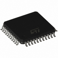
ST72C334J4T6 STMicroelectronics, ST72C334J4T6 Datasheet - Page 112

ST72C334J4T6
Manufacturer Part Number
ST72C334J4T6
Description
MCU 8BIT FLASH SPI SCI 44TQFP
Manufacturer
STMicroelectronics
Series
ST7r
Datasheet
1.ST72C124J2T6.pdf
(153 pages)
Specifications of ST72C334J4T6
Core Processor
ST7
Core Size
8-Bit
Speed
16MHz
Connectivity
SCI, SPI
Peripherals
LVD, POR, PWM, WDT
Number Of I /o
32
Program Memory Size
16KB (16K x 8)
Program Memory Type
FLASH
Eeprom Size
256 x 8
Ram Size
512 x 8
Voltage - Supply (vcc/vdd)
3.2 V ~ 5.5 V
Data Converters
A/D 6x8b
Oscillator Type
Internal
Operating Temperature
-40°C ~ 85°C
Package / Case
44-TQFP, 44-VQFP
Processor Series
ST72C3x
Core
ST7
Data Bus Width
8 bit
Data Ram Size
512 B
Interface Type
SCI, SPI
Maximum Clock Frequency
8 MHz
Number Of Programmable I/os
32
Number Of Timers
4 bit
Operating Supply Voltage
3.2 V to 5.5 V
Maximum Operating Temperature
+ 85 C
Mounting Style
SMD/SMT
Development Tools By Supplier
ST7C334-INDART, ST7MDT2-EPB2/US
Minimum Operating Temperature
- 40 C
On-chip Adc
8 bit
Lead Free Status / RoHS Status
Lead free / RoHS Compliant
Other names
497-4838
Available stocks
Company
Part Number
Manufacturer
Quantity
Price
Company:
Part Number:
ST72C334J4T6
Manufacturer:
STMicroelectronics
Quantity:
10 000
ST72334J/N, ST72314J/N, ST72124J
FUNCTIONAL OPERATING CONDITIONS (Cont’d)
Figure 60. High LVD Threshold Versus V
Figure 61. Medium LVD Threshold Versus V
Figure 62. Low LVD Threshold Versus V
Notes:
1. LVD typical data are based on T
2. The minimum V
3. If the low LVD threshold is selected, when V
anteed to continue functioning until it goes into reset state. The specified V
on phase, but during a power down phase or voltage drop the device will function below this min. level.
112/153
DEVICE UNDER
DEVICE UNDER
DEVICE UNDER
IN THIS AREA
IN THIS AREA
IN THIS AREA
RESET
RESET
RESET
DD
f
f
f
OSC
OSC
OSC
rise time rate is needed to insure a correct device power-on and LVD reset. Not tested in production.
16
16
16
8
0
8
0
8
0
[MHz]
[MHz]
[MHz]
2.5
2.5
2.5
V
IT-
A
=25°C. They are given only as design guidelines and are not tested.
3
3
3.00V
V
IT-
DD
3.5
3.5
3.5V
DD
falls below 3.2V, (V
DD
V
IT-
and f
and f
DD
3.85
and f
OSC
OSC
4
4
4
OSC
for ROM devices
for ROM devices
for ROM devices
DD
4.5
4.5
4.5
minimum operating voltage), the device is guar-
DD
min. value is necessary in the device power
5
5
5
2)3)
2)
2)
5.5
5.5
5.5
SUPPLY VOLTAGE [V]
SUPPLY VOLTAGE [V]
SUPPLY VOLTAGE [V]
FUNCTIONAL AREA
FUNCTIONAL AREA
FUNCTIONAL AREA
FUNCTIONALITY
NOT GUARANTEED
IN THIS AREA
FUNCTIONALITY
NOT GUARANTEED
IN THIS AREA
FUNCTIONALITY
NOT GUARANTEED
IN THIS AREA


