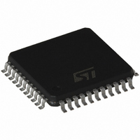
ST72C334J4T6 STMicroelectronics, ST72C334J4T6 Datasheet - Page 89

ST72C334J4T6
Manufacturer Part Number
ST72C334J4T6
Description
MCU 8BIT FLASH SPI SCI 44TQFP
Manufacturer
STMicroelectronics
Series
ST7r
Datasheet
1.ST72C124J2T6.pdf
(153 pages)
Specifications of ST72C334J4T6
Core Processor
ST7
Core Size
8-Bit
Speed
16MHz
Connectivity
SCI, SPI
Peripherals
LVD, POR, PWM, WDT
Number Of I /o
32
Program Memory Size
16KB (16K x 8)
Program Memory Type
FLASH
Eeprom Size
256 x 8
Ram Size
512 x 8
Voltage - Supply (vcc/vdd)
3.2 V ~ 5.5 V
Data Converters
A/D 6x8b
Oscillator Type
Internal
Operating Temperature
-40°C ~ 85°C
Package / Case
44-TQFP, 44-VQFP
Processor Series
ST72C3x
Core
ST7
Data Bus Width
8 bit
Data Ram Size
512 B
Interface Type
SCI, SPI
Maximum Clock Frequency
8 MHz
Number Of Programmable I/os
32
Number Of Timers
4 bit
Operating Supply Voltage
3.2 V to 5.5 V
Maximum Operating Temperature
+ 85 C
Mounting Style
SMD/SMT
Development Tools By Supplier
ST7C334-INDART, ST7MDT2-EPB2/US
Minimum Operating Temperature
- 40 C
On-chip Adc
8 bit
Lead Free Status / RoHS Status
Lead free / RoHS Compliant
Other names
497-4838
Available stocks
Company
Part Number
Manufacturer
Quantity
Price
Company:
Part Number:
ST72C334J4T6
Manufacturer:
STMicroelectronics
Quantity:
10 000
SERIAL COMMUNICATIONS INTERFACE (Cont’d)
14.5.5.3 Receiver
The SCI can receive data words of either 8 or 9
bits. When the M bit is set, word length is 9 bits
and the MSB is stored in the R8 bit in the CR1 reg-
ister.
Character reception
During a SCI reception, data shifts in least signifi-
cant bit first through the RDI pin. In this mode, DR
register consists in a buffer (RDR) between the in-
ternal bus and the received shift register (see Fig-
ure 1.).
Procedure
– Select the M bit to define the word length.
– Select the desired baud rate using the BRR and
– Set the RE bit, this enables the receiver which
When a character is received:
– The RDRF bit is set. It indicates that the content
– An interrupt is generated if the RIE bit is set and
– The error flags can be set if a frame error, noise
Clearing the RDRF bit is performed by the following
software sequence done by:
1. An access to the SR register
2. A read to the DR register.
The RDRF bit must be cleared before the end of the
reception of the next character to avoid an overrun
error.
Break Character
When a break character is received, the SCI han-
dles it as a framing error.
Idle Character
When a idle frame is detected, there is the same
procedure as a data received character plus an in-
terrupt if the ILIE bit is set and the I bit is cleared in
the CCR register.
the ERPR registers.
begins searching for a start bit.
of the shift register is transferred to the RDR.
the I bit is cleared in the CCR register.
or an overrun error has been detected during re-
ception.
Overrun Error
An overrun error occurs when a character is re-
ceived when RDRF has not been reset. Data can
not be transferred from the shift register to the
TDR register as long as the RDRF bit is not
cleared.
When a overrun error occurs:
– The OR bit is set.
– The RDR content will not be lost.
– The shift register will be overwritten.
– An interrupt is generated if the RIE bit is set and
The OR bit is reset by an access to the SR register
followed by a DR register read operation.
Noise Error
Oversampling techniques are used for data recov-
ery by discriminating between valid incoming data
and noise.
When noise is detected in a frame:
– The NF is set at the rising edge of the RDRF bit.
– Data is transferred from the Shift register to the
– No interrupt is generated. However this bit rises
The NF bit is reset by a SR register read operation
followed by a DR register read operation.
Framing Error
A framing error is detected when:
– The stop bit is not recognized on reception at the
– A break is received.
When the framing error is detected:
– the FE bit is set by hardware
– Data is transferred from the Shift register to the
– No interrupt is generated. However this bit rises
The FE bit is reset by a SR register read operation
followed by a DR register read operation.
the I bit is cleared in the CCR register.
DR register.
at the same time as the RDRF bit which itself
generates an interrupt.
expected time, following either a de-synchroni-
zation or excessive noise.
DR register.
at the same time as the RDRF bit which itself
generates an interrupt.
ST72334J/N, ST72314J/N, ST72124J
89/153


