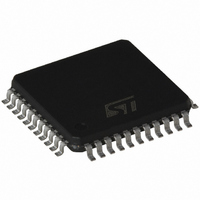
ST72C334J4T6 STMicroelectronics, ST72C334J4T6 Datasheet - Page 68

ST72C334J4T6
Manufacturer Part Number
ST72C334J4T6
Description
MCU 8BIT FLASH SPI SCI 44TQFP
Manufacturer
STMicroelectronics
Series
ST7r
Datasheet
1.ST72C124J2T6.pdf
(153 pages)
Specifications of ST72C334J4T6
Core Processor
ST7
Core Size
8-Bit
Speed
16MHz
Connectivity
SCI, SPI
Peripherals
LVD, POR, PWM, WDT
Number Of I /o
32
Program Memory Size
16KB (16K x 8)
Program Memory Type
FLASH
Eeprom Size
256 x 8
Ram Size
512 x 8
Voltage - Supply (vcc/vdd)
3.2 V ~ 5.5 V
Data Converters
A/D 6x8b
Oscillator Type
Internal
Operating Temperature
-40°C ~ 85°C
Package / Case
44-TQFP, 44-VQFP
Processor Series
ST72C3x
Core
ST7
Data Bus Width
8 bit
Data Ram Size
512 B
Interface Type
SCI, SPI
Maximum Clock Frequency
8 MHz
Number Of Programmable I/os
32
Number Of Timers
4 bit
Operating Supply Voltage
3.2 V to 5.5 V
Maximum Operating Temperature
+ 85 C
Mounting Style
SMD/SMT
Development Tools By Supplier
ST7C334-INDART, ST7MDT2-EPB2/US
Minimum Operating Temperature
- 40 C
On-chip Adc
8 bit
Lead Free Status / RoHS Status
Lead free / RoHS Compliant
Other names
497-4838
Available stocks
Company
Part Number
Manufacturer
Quantity
Price
Company:
Part Number:
ST72C334J4T6
Manufacturer:
STMicroelectronics
Quantity:
10 000
ST72334J/N, ST72314J/N, ST72124J
16-BIT TIMER (Cont’d)
CONTROL REGISTER 2 (CR2)
Read/Write
Reset Value: 0000 0000 (00h)
Bit 7 = OC1E Output Compare 1 Pin Enable.
This bit is used only to output the signal from the
timer on the OCMP1 pin (OLV1 in Output Com-
pare mode, both OLV1 and OLV2 in PWM and
one-pulse mode). Whatever the value of the OC1E
bit, the internal Output Compare 1 function of the
timer remains active.
0: OCMP1 pin alternate function disabled (I/O pin
1: OCMP1 pin alternate function enabled.
Bit 6 = OC2E Output Compare 2 Pin Enable.
This bit is used only to output the signal from the
timer on the OCMP2 pin (OLV2 in Output Com-
pare mode). Whatever the value of the OC2E bit,
the internal Output Compare 2 function of the timer
remains active.
0: OCMP2 pin alternate function disabled (I/O pin
1: OCMP2 pin alternate function enabled.
Bit 5 = OPM One Pulse mode.
0: One Pulse mode is not active.
1: One Pulse mode is active, the ICAP1 pin can be
68/153
OC1E OC2E OPM PWM CC1 CC0 IEDG2 EXEDG
free for general-purpose I/O).
free for general-purpose I/O).
used to trigger one pulse on the OCMP1 pin; the
active transition is given by the IEDG1 bit. The
length of the generated pulse depends on the
contents of the OC1R register.
7
0
Bit 4 = PWM Pulse Width Modulation.
0: PWM mode is not active.
1: PWM mode is active, the OCMP1 pin outputs a
Bits 3:2 = CC[1:0] Clock Control.
The timer clock mode depends on these bits:
Table 14. Clock Control Bits
Note: If the external clock pin is not available, pro-
gramming the external clock configuration stops
the counter.
Bit 1 = IEDG2 Input Edge 2.
This bit determines which type of level transition
on the ICAP2 pin will trigger the capture.
0: A falling edge triggers the capture.
1: A rising edge triggers the capture.
Bit 0 = EXEDG External Clock Edge.
This bit determines which type of level transition
on the external clock pin (EXTCLK) will trigger the
counter register.
0: A falling edge triggers the counter register.
1: A rising edge triggers the counter register.
External Clock (where
programmable cyclic signal; the length of the
pulse depends on the value of OC1R register;
the period depends on the value of OC2R regis-
ter.
Timer Clock
available)
f
f
f
CPU
CPU
CPU
/ 4
/ 2
/ 8
CC1
0
0
1
1
CC0
0
1
0
1


