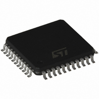
ST72C334J4T6 STMicroelectronics, ST72C334J4T6 Datasheet - Page 50

ST72C334J4T6
Manufacturer Part Number
ST72C334J4T6
Description
MCU 8BIT FLASH SPI SCI 44TQFP
Manufacturer
STMicroelectronics
Series
ST7r
Datasheet
1.ST72C124J2T6.pdf
(153 pages)
Specifications of ST72C334J4T6
Core Processor
ST7
Core Size
8-Bit
Speed
16MHz
Connectivity
SCI, SPI
Peripherals
LVD, POR, PWM, WDT
Number Of I /o
32
Program Memory Size
16KB (16K x 8)
Program Memory Type
FLASH
Eeprom Size
256 x 8
Ram Size
512 x 8
Voltage - Supply (vcc/vdd)
3.2 V ~ 5.5 V
Data Converters
A/D 6x8b
Oscillator Type
Internal
Operating Temperature
-40°C ~ 85°C
Package / Case
44-TQFP, 44-VQFP
Processor Series
ST72C3x
Core
ST7
Data Bus Width
8 bit
Data Ram Size
512 B
Interface Type
SCI, SPI
Maximum Clock Frequency
8 MHz
Number Of Programmable I/os
32
Number Of Timers
4 bit
Operating Supply Voltage
3.2 V to 5.5 V
Maximum Operating Temperature
+ 85 C
Mounting Style
SMD/SMT
Development Tools By Supplier
ST7C334-INDART, ST7MDT2-EPB2/US
Minimum Operating Temperature
- 40 C
On-chip Adc
8 bit
Lead Free Status / RoHS Status
Lead free / RoHS Compliant
Other names
497-4838
Available stocks
Company
Part Number
Manufacturer
Quantity
Price
Company:
Part Number:
ST72C334J4T6
Manufacturer:
STMicroelectronics
Quantity:
10 000
ST72334J/N, ST72314J/N, ST72124J
WATCHDOG TIMER (Cont’d)
The application program must write in the CR reg-
ister at regular intervals during normal operation to
prevent an MCU reset. The value to be stored in
the CR register must be between FFh and C0h
(see
– The WDGA bit is set (watchdog enabled)
– The T6 bit is set to prevent generating an imme-
– The T[5:0] bits contain the number of increments
Table 11.Watchdog Timing (f
Notes: Following a reset, the watchdog is disa-
bled. Once activated it cannot be disabled, except
by a reset.
The T6 bit can be used to generate a software re-
set (the WDGA bit is set and the T6 bit is cleared).
If the watchdog is activated, the HALT instruction
will generate a Reset.
14.1.4 Hardware Watchdog Option
If Hardware Watchdog is selected by option byte,
the watchdog is always active and the WDGA bit in
the CR is not used.
Refer to the device-specific Option Byte descrip-
tion.
14.1.5 Low Power Modes
14.1.6 Interrupts
None.
50/153
Mode
WAIT
HALT
diate reset
which represents the time delay before the
watchdog produces a reset.
Max
Min
Table 11 .Watchdog Timing (fCPU = 8
Description
No effect on Watchdog.
Immediate reset generation as soon as
the HALT instruction is executed if the
Watchdog is activated (WDGA bit is
set).
CR Register
initial value
C0h
FFh
WDG timeout period
CPU
= 8 MHz)
98.304
1.536
(ms)
MHz)):
14.1.7 Register Description
CONTROL REGISTER (CR)
Read /Write
Reset Value: 0111 1111 (7Fh)
Bit 7 = WDGA Activation bit .
This bit is set by software and only cleared by
hardware after a reset. When WDGA = 1, the
watchdog can generate a reset.
0: Watchdog disabled
1: Watchdog enabled
Note: This bit is not used if the hardware watch-
dog option is enabled by option byte.
Bit 6:0 = T[6:0] 7-bit timer (MSB to LSB).
These bits contain the decremented value. A reset
is produced when it rolls over from 40h to 3Fh (T6
becomes cleared).
STATUS REGISTER (SR)
Read /Write
Reset Value*: 0000 0000 (00h)
Bit 0 = WDOGF Watchdog flag .
This bit is set by a watchdog reset and cleared by
software or a power on/off reset. This bit is useful
for distinguishing power/on off or external reset
and watchdog reset.
0: No Watchdog reset occurred
1: Watchdog reset occurred
* Only by software and power on/off reset
Note: This register is not used in versions without
LVD Reset.
WDGA
7
-
7
-
T6
-
T5
-
T4
-
T3
-
T2
-
T1
WDOGF
0
T0
0


