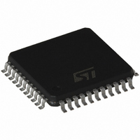
ST72C334J4T6 STMicroelectronics, ST72C334J4T6 Datasheet - Page 74

ST72C334J4T6
Manufacturer Part Number
ST72C334J4T6
Description
MCU 8BIT FLASH SPI SCI 44TQFP
Manufacturer
STMicroelectronics
Series
ST7r
Datasheet
1.ST72C124J2T6.pdf
(153 pages)
Specifications of ST72C334J4T6
Core Processor
ST7
Core Size
8-Bit
Speed
16MHz
Connectivity
SCI, SPI
Peripherals
LVD, POR, PWM, WDT
Number Of I /o
32
Program Memory Size
16KB (16K x 8)
Program Memory Type
FLASH
Eeprom Size
256 x 8
Ram Size
512 x 8
Voltage - Supply (vcc/vdd)
3.2 V ~ 5.5 V
Data Converters
A/D 6x8b
Oscillator Type
Internal
Operating Temperature
-40°C ~ 85°C
Package / Case
44-TQFP, 44-VQFP
Processor Series
ST72C3x
Core
ST7
Data Bus Width
8 bit
Data Ram Size
512 B
Interface Type
SCI, SPI
Maximum Clock Frequency
8 MHz
Number Of Programmable I/os
32
Number Of Timers
4 bit
Operating Supply Voltage
3.2 V to 5.5 V
Maximum Operating Temperature
+ 85 C
Mounting Style
SMD/SMT
Development Tools By Supplier
ST7C334-INDART, ST7MDT2-EPB2/US
Minimum Operating Temperature
- 40 C
On-chip Adc
8 bit
Lead Free Status / RoHS Status
Lead free / RoHS Compliant
Other names
497-4838
Available stocks
Company
Part Number
Manufacturer
Quantity
Price
Company:
Part Number:
ST72C334J4T6
Manufacturer:
STMicroelectronics
Quantity:
10 000
ST72334J/N, ST72314J/N, ST72124J
SERIAL PERIPHERAL INTERFACE (Cont’d)
14.4.4 Functional Description
Figure 42
(SPI) block diagram.
This interface contains 3 dedicated registers:
Refer to the CR, SR and DR registers in
14.4.7for the bit definitions.
14.4.4.1 Master Configuration
In a master configuration, the serial clock is gener-
ated on the SCK pin.
Procedure
74/153
– A Control Register (CR)
– A Status Register (SR)
– A Data Register (DR)
– Select the SPR0 & SPR1 bits to define the se-
– Select the CPOL and CPHA bits to define one
– The SS pin must be connected to a high level
– The MSTR and SPE bits must be set (they re-
rial clock baud rate (see CR register).
of the four relationships between the data
transfer and the serial clock (see
signal during the complete byte transmit se-
quence.
main set only if the SS pin is connected to a
high level signal).
shows the serial peripheral interface
Figure
Section
45).
During the last clock cycle the SPIF bit is set, a
copy of the data byte received in the shift register
is moved to a buffer. When the DR register is read,
the SPI peripheral returns this buffered value.
Clearing the SPIF bit is performed by the following
software sequence:
1. An access to the SR register while the SPIF bit
2. A read to the DR register.
Note: While the SPIF bit is set, all writes to the DR
register are inhibited until the SR register is read.
In this configuration the MOSI pin is a data output
and to the MISO pin is a data input.
Transmit sequence
The transmit sequence begins when a byte is writ-
ten the DR register.
The data byte is parallel loaded into the 8-bit shift
register (from the internal bus) during a write cycle
and then shifted out serially to the MOSI pin most
significant bit first.
When data transfer is complete:
– The SPIF bit is set by hardware
– An interrupt is generated if the SPIE bit is set
is set
and the I bit in the CCR register is cleared.


