ST72C334J4T6 STMicroelectronics, ST72C334J4T6 Datasheet - Page 28

ST72C334J4T6
Manufacturer Part Number
ST72C334J4T6
Description
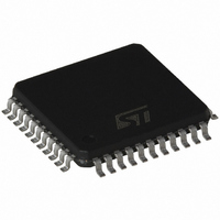
MCU 8BIT FLASH SPI SCI 44TQFP
Manufacturer
STMicroelectronics
Series
ST7r
Datasheet
1.ST72C124J2T6.pdf
(153 pages)
Specifications of ST72C334J4T6
Core Processor
ST7
Core Size
8-Bit
Speed
16MHz
Connectivity
SCI, SPI
Peripherals
LVD, POR, PWM, WDT
Number Of I /o
32
Program Memory Size
16KB (16K x 8)
Program Memory Type
FLASH
Eeprom Size
256 x 8
Ram Size
512 x 8
Voltage - Supply (vcc/vdd)
3.2 V ~ 5.5 V
Data Converters
A/D 6x8b
Oscillator Type
Internal
Operating Temperature
-40°C ~ 85°C
Package / Case
44-TQFP, 44-VQFP
Processor Series
ST72C3x
Core
ST7
Data Bus Width
8 bit
Data Ram Size
512 B
Interface Type
SCI, SPI
Maximum Clock Frequency
8 MHz
Number Of Programmable I/os
32
Number Of Timers
4 bit
Operating Supply Voltage
3.2 V to 5.5 V
Maximum Operating Temperature
+ 85 C
Mounting Style
SMD/SMT
Development Tools By Supplier
ST7C334-INDART, ST7MDT2-EPB2/US
Minimum Operating Temperature
- 40 C
On-chip Adc
8 bit
Lead Free Status / RoHS Status
Lead free / RoHS Compliant
Other names
497-4838
Available stocks
Company
Part Number
Manufacturer
Quantity
Price
Company:
Part Number:
ST72C334J4T6
Manufacturer:
STMicroelectronics
Quantity:
10 000
ST72334J/N, ST72314J/N, ST72124J
9.2 RESET SEQUENCE MANAGER (RSM)
9.2.1 Introduction
The reset sequence manager includes three RE-
SET sources as shown in
These sources act on the RESET pin and it is al-
ways kept low during the delay phase.
The RESET service routine vector is fixed at ad-
dresses FFFEh-FFFFh in the ST7 memory map.
The basic RESET sequence consists of 3 phases
as shown in
Figure 15. Reset Block Diagram
28/153
External RESET source pulse
Internal LVD RESET (Low Voltage Detection)
Internal WATCHDOG RESET
Delay depending on the RESET source
4096 CPU clock cycle delay
RESET vector fetch
RESET
Figure
14:
Figure
V
DD
R
ON
15:
f
CPU
The 4096 CPU clock cycle delay allows the oscil-
lator to stabilise and ensures that recovery has
taken place from the Reset state.
The RESET vector fetch phase duration is 2 clock
cycles.
Figure 14. RESET Sequence Phases
DELAY
4096 CLOCK CYCLES
INTERNAL RESET
RESET
WATCHDOG RESET
LVD RESET
INTERNAL
RESET
VECTOR
FETCH


