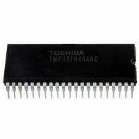
TMP86FH46ANG(Z) Toshiba, TMP86FH46ANG(Z) Datasheet - Page 110

TMP86FH46ANG(Z)
Manufacturer Part Number
TMP86FH46ANG(Z)
Description
IC MCU 8BIT FLASH 16KB 42-SDIP
Manufacturer
Toshiba
Series
TLCS-870/Cr
Datasheet
1.TMP86FH46ANGZ.pdf
(214 pages)
Specifications of TMP86FH46ANG(Z)
Core Processor
870/C
Core Size
8-Bit
Speed
16MHz
Connectivity
SIO, UART/USART
Peripherals
LED, PWM, WDT
Number Of I /o
33
Program Memory Size
16KB (16K x 8)
Program Memory Type
FLASH
Ram Size
512 x 8
Voltage - Supply (vcc/vdd)
2.7 V ~ 5.5 V
Data Converters
A/D 8x10b
Oscillator Type
Internal
Operating Temperature
-40°C ~ 85°C
Package / Case
42-SDIP (0.600", 15.24mm)
Processor Series
TLCS-870
Core
870/C
Data Bus Width
8 bit
Data Ram Size
512 B
Interface Type
SIO, UART
Maximum Clock Frequency
16 MHz
Number Of Programmable I/os
33
Number Of Timers
3
Maximum Operating Temperature
+ 85 C
Mounting Style
Through Hole
Development Tools By Supplier
BMSKTOPAS86FH47(AND), BM1040R0A, BMP86A100010A, BMP86A100010B, BMP86A200010B, BMP86A200020A, BMP86A300010A, BMP86A300020A, BMP86A300030A, SW89CN0-ZCC, SW00MN0-ZCC
Minimum Operating Temperature
- 40 C
On-chip Adc
10 bit, 8 Channel
For Use With
BM1401W0A-G - FLASH WRITER ON-BOARD PROGRAMTMP86C909XB - EMULATION CHIP FOR TMP86F SDIP
Lead Free Status / RoHS Status
Lead free / RoHS Compliant
Eeprom Size
-
Lead Free Status / Rohs Status
Details
Other names
TMP86FH46ANGZ
9.1 Configuration
9.3.6 16-Bit Event Counter Mode (TC3 and 4)
9.3.7 16-Bit Pulse Width Modulation (PWM) Output Mode (TC3 and 4)
TimerCounter 3 and 4 are cascadable to form the 16-bit PWM signal generator.
logic level output from the timer F/F4 is switched to the opposite state. The counter continues counting. The
logic level output from the timer F/F4 is switched to the opposite state again by the counter overflow, and the
counter is cleared. The INTTC4 interrupt is generated at this time.
mum frequency to be supplied is fc/2
SLEEP1/2 mode.
generated. Upon reset, the timer F/F4 is cleared to 0.
PWREG4 and 3 can be changed while the timer is running. The values set to PWREG4 and 3 during a run of
the timer are shifted by the INTTCj interrupt request and loaded into PWREG4 and 3. While the timer is
stopped, the values are shifted immediately after the programming of PWREG4 and 3. Set the lower byte
(PWREG3) and upper byte (PWREG3) in this order to program PWREG4 and 3. (Programming only the lower
or upper byte of the register should not be attempted.)
read, but not the values set in PWREG4 and 3. Therefore, after writing to the PWREG4 and 3, reading data of
PWREG4 and 3 is previous value until INTTC4 is generated.
and 4 are cascadable to form a 16-bit event counter.
the timer is started by setting TC4CR<TC4S> to 1, an INTTC4 interrupt is generated and the up-counter is
cleared.
Two machine cycles are required for the low- or high-level pulse input to the TC3 pin.
the SLOW1/2 or SLEEP1/2 mode. Program the lower byte (TTREG3), and upper byte (TTREG4) in this
order in the timer register. (Programming only the upper or lower byte should not be attempted.)
This mode is used to generate a pulse-width modulated (PWM) signals with up to 16 bits of resolution. The
The counter counts up using the internal clock or external clock.
When a match between the up-counter and the timer register (PWREG3, PWREG4) value is detected, the
Two machine cycles are required for the high- or low-level pulse input to the TC3 pin. Therefore, a maxi-
Since the initial value can be set to the timer F/F4 by TC4CR<TFF4>, positive and negative pulses can be
(The logic level output from the
Since PWREG4 and 3 in the PWM mode are serially connected to the shift register, the values set to
If executing the read instruction to PWREG4 and 3 during PWM output, the values set in the shift register is
For the pin used for PWM output, the output latch of the I/O port must be set to 1.
Note 1: In the PWM mode, program the timer register PWREG4 and 3 immediately after the INTTC4 interrupt
Note 2: When the timer is stopped during PWM output, the
Note 1:
Note 2:
Note 3:
In the event counter mode, the up-counter counts up at the falling edge to the TC3 pin. The TimerCounter 3
When a match between the up-counter and the timer register (TTREG3, TTREG4) value is detected after
After being cleared, the up-counter restarts counting at the falling edge of the input pulse to the TC3 pin.
Therefore, a maximum frequency to be supplied is fc/2
request is generated (normally in the INTTC4 interrupt service routine.) If the programming of PWREGj and
the interrupt request occur at the same time, an unstable value is shifted, that may result in generation of
pulse different from the programmed value until the next INTTC4 interrupt request is generated.
stopped. To change the output status, program TC4CR<TFF4> after the timer is stopped. Do not program
TC4CR<TFF4> upon stopping of the timer.
Example: Fixing the
In the event counter mode, fix TCjCR<TFFj> to 0. If not fixed, the
In the event counter mode, do not change the TTREGj setting while the timer is running. Since TTREGj is not in
the shift register configuration in the event counter mode, the new value programmed in TTREGj is in effect imme-
diately after the programming. Therefore, if TTREGj is changed while the timer is running, an expected operation
may not be obtained.
j = 3, 4
PWM
4 pin to the high level when the TimerCounter is stopped
PWM
4
Hz in the NORMAL1 or IDLE1 mode, and fs/2
4 pin is the opposite to the timer F/F4 logic level.)
Page 96
PWM
4
4 pin holds the output status when the timer is
Hz in the NORMAL1 or IDLE1 mode, and fs/2
PDOj, PWMj
and
PPGj
4
pins may output pulses.
to in the SLOW1/2 or
TMP86FH46ANG
4
in


