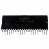
TMP86FH46ANG(Z) Toshiba, TMP86FH46ANG(Z) Datasheet - Page 79

TMP86FH46ANG(Z)
Manufacturer Part Number
TMP86FH46ANG(Z)
Description
IC MCU 8BIT FLASH 16KB 42-SDIP
Manufacturer
Toshiba
Series
TLCS-870/Cr
Datasheet
1.TMP86FH46ANGZ.pdf
(214 pages)
Specifications of TMP86FH46ANG(Z)
Core Processor
870/C
Core Size
8-Bit
Speed
16MHz
Connectivity
SIO, UART/USART
Peripherals
LED, PWM, WDT
Number Of I /o
33
Program Memory Size
16KB (16K x 8)
Program Memory Type
FLASH
Ram Size
512 x 8
Voltage - Supply (vcc/vdd)
2.7 V ~ 5.5 V
Data Converters
A/D 8x10b
Oscillator Type
Internal
Operating Temperature
-40°C ~ 85°C
Package / Case
42-SDIP (0.600", 15.24mm)
Processor Series
TLCS-870
Core
870/C
Data Bus Width
8 bit
Data Ram Size
512 B
Interface Type
SIO, UART
Maximum Clock Frequency
16 MHz
Number Of Programmable I/os
33
Number Of Timers
3
Maximum Operating Temperature
+ 85 C
Mounting Style
Through Hole
Development Tools By Supplier
BMSKTOPAS86FH47(AND), BM1040R0A, BMP86A100010A, BMP86A100010B, BMP86A200010B, BMP86A200020A, BMP86A300010A, BMP86A300020A, BMP86A300030A, SW89CN0-ZCC, SW00MN0-ZCC
Minimum Operating Temperature
- 40 C
On-chip Adc
10 bit, 8 Channel
For Use With
BM1401W0A-G - FLASH WRITER ON-BOARD PROGRAMTMP86C909XB - EMULATION CHIP FOR TMP86F SDIP
Lead Free Status / RoHS Status
Lead free / RoHS Compliant
Eeprom Size
-
Lead Free Status / Rohs Status
Details
Other names
TMP86FH46ANGZ
- Current page: 79 of 214
- Download datasheet (3Mb)
7.4 Port P3 (P37 to P30)
(000EH)
(0003H)
control. Port P3 is also used as an analog input, key on wake up input. Input/output mode is specified by the corre-
sponding bit in the port P3 input/output control register (P3CR), and ADCCR1<AINDS>. During reset, P3CR are
initialized to “0” and ADCCR1<AINDS> is set to “1”, therefore port P3 is configured as an input.
“0”. When ADCCR1<AINDS> is “0”, the pin which is specified as an analog input is used as analog input indepen-
dent on the value of P3CR and P3DR.
ifying as an analog input.
input is read “0”. and the data of port which is not selected as an analog input is read “0” or “1”, depend on the volt-
age level.
Data can be written into the output latch regardless of P3CR contents, therefore initial output data should be written
into the output latch before setting P3CR.
cuted to keep a precision. In addition, a variable signal should not be input to an adjacent port to the analog input
during AD conversion.
P3DR
P3CR
R/W
Port P3 is an 8-bit input/output port which can be configured as an input or an output in one-bit unit under software
When used as an analog input, set an analog input channel to ADCCR1<SAIN> and clear ADCCR1<AINDS> to
When used as an input port or key on wake up input, the corresponding bit of P3CR is cleared to “0” without spec-
When the AD converter is enabled (ADCCR1<AINDS> is “0”), the data of port which is selected as an analog
When used as an output port, the corresponding bit of P3CR is set to “1” without specifying as an analog input.
The pins not used as analog input can be used as an input/output port. But output instructions should not be exe-
Note: Ports set to the input mode read the pin states. Ports set to the output mode read the output latch. When input pin and out-
put pin exist in port P3 together, the contents of the output latch which is specified as an input mode may be rewritten by
executing the bit manipulation instructions.
STOP5
AIN7
P37
P3CR
7
7
Data output (P3DR)
STOP4
Data input (P3DR)
AIN6
P36
6
6
I/O control
(Specified for each bit)
Key on wake up
Analog input
P3CRi input
STOP3
AIN5
OUTEN
P35
AINDS
STOPj
P3CRi
5
5
STOP
SAIN
STOP2
AIN4
P34
4
4
Output latch
Output latch
Figure 7-5 Port P3
D
D
AIN3
P33
0: Input mode
1: Output mode
Q
Q
3
3
Page 65
AIN2
P32
2
2
AIN1
P31
1
1
AIN0
P30
0
0
(Initial value: 0000 0000)
(Initial value: 0000 0000)
Note: i = 7
j = 5 to 2
P3i
to
0
TMP86FH46ANG
R/W
Related parts for TMP86FH46ANG(Z)
Image
Part Number
Description
Manufacturer
Datasheet
Request
R
Part Number:
Description:
Toshiba Semiconductor [TOSHIBA IGBT Module Silicon N Channel IGBT]
Manufacturer:
TOSHIBA Semiconductor CORPORATION
Datasheet:
Part Number:
Description:
TOSHIBA GTR MODULE SILICON NPN TRIPLE DIFFUSED TYPE
Manufacturer:
TOSHIBA Semiconductor CORPORATION
Datasheet:
Part Number:
Description:
TOSHIBA GTR Module Silicon N Channel IGBT
Manufacturer:
TOSHIBA Semiconductor CORPORATION
Datasheet:
Part Number:
Description:
TOSHIBA Intelligent Power Module Silicon N Channel IGBT
Manufacturer:
TOSHIBA Semiconductor CORPORATION
Datasheet:
Part Number:
Description:
TOSHIBA INTELLIGENT POWER MODULE SILICON N CHANNEL LGBT
Manufacturer:
TOSHIBA Semiconductor CORPORATION
Datasheet:
Part Number:
Description:
TOSHIBA IGBT Module Silicon N Channel IGBT
Manufacturer:
TOSHIBA Semiconductor CORPORATION
Datasheet:
Part Number:
Description:
TOSHIBA GTR MODULE SILICON N−CHANNEL IGBT
Manufacturer:
TOSHIBA Semiconductor CORPORATION
Datasheet:
Part Number:
Description:
TOSHIBA Intelligent Power Module Silicon N Channel IGBT
Manufacturer:
TOSHIBA Semiconductor CORPORATION
Datasheet:
Part Number:
Description:
TOSHIBA GTR Module Silicon N Channel IGBT
Manufacturer:
TOSHIBA Semiconductor CORPORATION
Datasheet:
Part Number:
Description:
TOSHIBA INTELLIGENT POWER MODULE
Manufacturer:
TOSHIBA Semiconductor CORPORATION
Datasheet:
Part Number:
Description:
TOSHIBA Intelligent Power Module Silicon N Channel IGBT
Manufacturer:
TOSHIBA Semiconductor CORPORATION
Datasheet:
Part Number:
Description:
TOSHIBA Intelligent Power Module Silicon N Channel IGBT
Manufacturer:
TOSHIBA Semiconductor CORPORATION
Datasheet:
Part Number:
Description:
TOSHIBA IGBT Module Silicon N Channel IGBT
Manufacturer:
TOSHIBA Semiconductor CORPORATION
Datasheet:
Part Number:
Description:
TOSHIBA Intelligent Power Module Silicon N Channel IGBT
Manufacturer:
TOSHIBA Semiconductor CORPORATION
Datasheet:
Part Number:
Description:
Toshiba Semiconductor [SILICON N CHANNEL 1GBT]
Manufacturer:
TOSHIBA Semiconductor CORPORATION
Datasheet:


