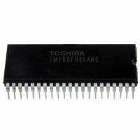
TMP86FH46ANG(Z) Toshiba, TMP86FH46ANG(Z) Datasheet - Page 194

TMP86FH46ANG(Z)
Manufacturer Part Number
TMP86FH46ANG(Z)
Description
IC MCU 8BIT FLASH 16KB 42-SDIP
Manufacturer
Toshiba
Series
TLCS-870/Cr
Datasheet
1.TMP86FH46ANGZ.pdf
(214 pages)
Specifications of TMP86FH46ANG(Z)
Core Processor
870/C
Core Size
8-Bit
Speed
16MHz
Connectivity
SIO, UART/USART
Peripherals
LED, PWM, WDT
Number Of I /o
33
Program Memory Size
16KB (16K x 8)
Program Memory Type
FLASH
Ram Size
512 x 8
Voltage - Supply (vcc/vdd)
2.7 V ~ 5.5 V
Data Converters
A/D 8x10b
Oscillator Type
Internal
Operating Temperature
-40°C ~ 85°C
Package / Case
42-SDIP (0.600", 15.24mm)
Processor Series
TLCS-870
Core
870/C
Data Bus Width
8 bit
Data Ram Size
512 B
Interface Type
SIO, UART
Maximum Clock Frequency
16 MHz
Number Of Programmable I/os
33
Number Of Timers
3
Maximum Operating Temperature
+ 85 C
Mounting Style
Through Hole
Development Tools By Supplier
BMSKTOPAS86FH47(AND), BM1040R0A, BMP86A100010A, BMP86A100010B, BMP86A200010B, BMP86A200020A, BMP86A300010A, BMP86A300020A, BMP86A300030A, SW89CN0-ZCC, SW00MN0-ZCC
Minimum Operating Temperature
- 40 C
On-chip Adc
10 bit, 8 Channel
For Use With
BM1401W0A-G - FLASH WRITER ON-BOARD PROGRAMTMP86C909XB - EMULATION CHIP FOR TMP86F SDIP
Lead Free Status / RoHS Status
Lead free / RoHS Compliant
Eeprom Size
-
Lead Free Status / Rohs Status
Details
Other names
TMP86FH46ANGZ
- Current page: 194 of 214
- Download datasheet (3Mb)
15.13 Specifying the Erasure Area
15.13Specifying the Erasure Area
15.14Port Input Control Register
Erasure Area Specification Data (n−2 byte data)
the sector erase while the read protection is enabled results in an infinite loop.
read protection is disabled. Therefore, execute the chip erase (not sector erase) to disable the read protection.
to prevent overlap current to unused ports. (All port inputs and peripheral function inputs shared with the ports
become invalid.) Therefore, to access to the flash memory in the RAM loader mode without UART communication,
port inputs must be valid. To make port inputs valid, set the pin of the port input control register (SPCR) to “1”.
In the flash memory erasing mode, the erasure area of the flash memory is specified by n−2 byte data.
The start address of an erasure area is specified by ERASTA, and the end address is specified by ERAEND.
If ERASTA is equal to or smaller than ERAEND, the sector erase (erasure in 4 kbyte units) is executed. Executing
If ERASTA is larger than ERAEND, the chip erase (erasure of an entire flash memory area) is executed and the
Note: When the sector erase is executed for the area containing no flash cell, TMP86FH46ANG stops the UART commu-
In the serial PROM mode, the input level is fixed to the all ports except P03 and P02 ports with a hardware feature
The SPCR register is not operated in the MCU mode.
nication and enters the halt condition.
7
ERASTA
ERAEND
6
ERASTA
The start address of the
erasure area
The end address of the
erasure area
5
4
0000:
0001:
0010:
0011:
0100:
0101:
0110:
0111:
1000:
1001:
1010:
1011:
1100:
1101:
1110:
1111:
0000:
0001:
0010:
0011:
0100:
0101:
0110:
0111:
1000:
1001:
1010:
1011:
1100:
1101:
1110:
1111:
Page 180
3
from 0000H
from 1000H
from 2000H
from 3000H
from 4000H
from 5000H
from 6000H
from 7000H
from 8000H
from 9000H
from A000H
from B000H
from C000H
from D000H
from E000H
from F000H
to 0FFFH
to 1FFFH
to 2FFFH
to 3FFFH
to 4FFFH
to 5FFFH
to 6FFFH
to 7FFFH
to 8FFFH
to 9FFFH
to AFFFH
to BFFFH
to CFFFH
to DFFFH
to EFFFH
to FFFFH
2
ERAEND
1
0
TMP86FH46ANG
Related parts for TMP86FH46ANG(Z)
Image
Part Number
Description
Manufacturer
Datasheet
Request
R
Part Number:
Description:
Toshiba Semiconductor [TOSHIBA IGBT Module Silicon N Channel IGBT]
Manufacturer:
TOSHIBA Semiconductor CORPORATION
Datasheet:
Part Number:
Description:
TOSHIBA GTR MODULE SILICON NPN TRIPLE DIFFUSED TYPE
Manufacturer:
TOSHIBA Semiconductor CORPORATION
Datasheet:
Part Number:
Description:
TOSHIBA GTR Module Silicon N Channel IGBT
Manufacturer:
TOSHIBA Semiconductor CORPORATION
Datasheet:
Part Number:
Description:
TOSHIBA Intelligent Power Module Silicon N Channel IGBT
Manufacturer:
TOSHIBA Semiconductor CORPORATION
Datasheet:
Part Number:
Description:
TOSHIBA INTELLIGENT POWER MODULE SILICON N CHANNEL LGBT
Manufacturer:
TOSHIBA Semiconductor CORPORATION
Datasheet:
Part Number:
Description:
TOSHIBA IGBT Module Silicon N Channel IGBT
Manufacturer:
TOSHIBA Semiconductor CORPORATION
Datasheet:
Part Number:
Description:
TOSHIBA GTR MODULE SILICON N−CHANNEL IGBT
Manufacturer:
TOSHIBA Semiconductor CORPORATION
Datasheet:
Part Number:
Description:
TOSHIBA Intelligent Power Module Silicon N Channel IGBT
Manufacturer:
TOSHIBA Semiconductor CORPORATION
Datasheet:
Part Number:
Description:
TOSHIBA GTR Module Silicon N Channel IGBT
Manufacturer:
TOSHIBA Semiconductor CORPORATION
Datasheet:
Part Number:
Description:
TOSHIBA INTELLIGENT POWER MODULE
Manufacturer:
TOSHIBA Semiconductor CORPORATION
Datasheet:
Part Number:
Description:
TOSHIBA Intelligent Power Module Silicon N Channel IGBT
Manufacturer:
TOSHIBA Semiconductor CORPORATION
Datasheet:
Part Number:
Description:
TOSHIBA Intelligent Power Module Silicon N Channel IGBT
Manufacturer:
TOSHIBA Semiconductor CORPORATION
Datasheet:
Part Number:
Description:
TOSHIBA IGBT Module Silicon N Channel IGBT
Manufacturer:
TOSHIBA Semiconductor CORPORATION
Datasheet:
Part Number:
Description:
TOSHIBA Intelligent Power Module Silicon N Channel IGBT
Manufacturer:
TOSHIBA Semiconductor CORPORATION
Datasheet:
Part Number:
Description:
Toshiba Semiconductor [SILICON N CHANNEL 1GBT]
Manufacturer:
TOSHIBA Semiconductor CORPORATION
Datasheet:


