TMP86FH46ANG(Z) Toshiba, TMP86FH46ANG(Z) Datasheet - Page 123
TMP86FH46ANG(Z)
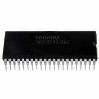
Manufacturer Part Number
TMP86FH46ANG(Z)
Description
IC MCU 8BIT FLASH 16KB 42-SDIP
Manufacturer
Toshiba
Series
TLCS-870/Cr
Datasheet
1.TMP86FH46ANGZ.pdf
(214 pages)
Specifications of TMP86FH46ANG(Z)
Core Processor
870/C
Core Size
8-Bit
Speed
16MHz
Connectivity
SIO, UART/USART
Peripherals
LED, PWM, WDT
Number Of I /o
33
Program Memory Size
16KB (16K x 8)
Program Memory Type
FLASH
Ram Size
512 x 8
Voltage - Supply (vcc/vdd)
2.7 V ~ 5.5 V
Data Converters
A/D 8x10b
Oscillator Type
Internal
Operating Temperature
-40°C ~ 85°C
Package / Case
42-SDIP (0.600", 15.24mm)
Processor Series
TLCS-870
Core
870/C
Data Bus Width
8 bit
Data Ram Size
512 B
Interface Type
SIO, UART
Maximum Clock Frequency
16 MHz
Number Of Programmable I/os
33
Number Of Timers
3
Maximum Operating Temperature
+ 85 C
Mounting Style
Through Hole
Development Tools By Supplier
BMSKTOPAS86FH47(AND), BM1040R0A, BMP86A100010A, BMP86A100010B, BMP86A200010B, BMP86A200020A, BMP86A300010A, BMP86A300020A, BMP86A300030A, SW89CN0-ZCC, SW00MN0-ZCC
Minimum Operating Temperature
- 40 C
On-chip Adc
10 bit, 8 Channel
For Use With
BM1401W0A-G - FLASH WRITER ON-BOARD PROGRAMTMP86C909XB - EMULATION CHIP FOR TMP86F SDIP
Lead Free Status / RoHS Status
Lead free / RoHS Compliant
Eeprom Size
-
Lead Free Status / Rohs Status
Details
Other names
TMP86FH46ANGZ


10.3.3 Transfer modes
10.3.2.3 Transmit/receive mode
10.3.3.1 Transmit mode
Transmit, receive and transmit/receive mode are selected by using SIOCR1<SIOM>.
(2)
(1)
(2)
(1)
Transmit mode is selected by writing “00B” to SIOCR1<SIOM>.
received sequentially beginning with the least significant bit (Bit0).
data is transferred sequentially beginning with the most significant bit (Bit7) and the data is received
sequentially beginning with the most significant (Bit7).
data is transferred sequentially beginning with the least significant bit (Bit0) and the data is received
sequentially beginning with the least significant (Bit0).
SIOCR1<SCK>. Transfer direction is selected by using SIOCR1<SIODIR>.
to “0”.
SCK
SIOCR1<SIODIR>, synchronizing with the
clock falling edge.
ferred to shift register, then the INTSIO interrupt request is generated, synchronizing with the next
falling edge on
LSB receive mode
LSB receive mode is selected by setting SIOCR1<SIODIR> to “1”, in which case the data is
MSB transmit/receive mode
MSB transmit/receive mode are selected by setting SIOCR1<SIODIR> to “0” in which case the
LSB transmit/receive mode
LSB transmit/receive mode are selected by setting SIOCR1<SIODIR> to “1”, in which case the
Starting the transmit operation
Transmit mode is selected by setting “00B” to SIOCR1<SIOM>. Serial clock is selected by using
When a transmit data is written to the transmit buffer register (SIOTDB), SIOSR<TXF> is cleared
After SIOCR1<SIOS> is set to “1”, SIOSR<SIOF> is set synchronously to “1” the falling edge of
The data is transferred sequentially starting from SO pin with the direction of the bit specified by
SIOSR<SEF> is kept in high level, between the first clock falling edge of
SIOSR<TXF> is set to “1” at the rising edge of pin after the data written to the SIOTDB is trans-
Note 1: In internal clock operation, when SIOCR1<SIOS> is set to "1", transfer mode does not start with-
Note 2: In internal clock operation, when the SIOCR1<SIOS> is set to "1", SIOTDB is transferred to shift
Note 3: In external clock operation, when the falling edge is input from
pin.
out writing a transmit data to the transmit buffer register (SIOTDB).
register after maximum 1-cycle of serial clock frequency, then a serial clock is output from
pin.
set to "1", SIOTDB is transferred to shift register immediately.
SCK
pin.
Page 109
SCK
pin's falling edge.
SCK
pin after SIOCR1<SIOS> is
SCK
TMP86FH46ANG
pin and eighth
SCK
Related parts for TMP86FH46ANG(Z)
Image
Part Number
Description
Manufacturer
Datasheet
Request
R

Part Number:
Description:
Toshiba Semiconductor [TOSHIBA IGBT Module Silicon N Channel IGBT]
Manufacturer:
TOSHIBA Semiconductor CORPORATION
Datasheet:
Part Number:
Description:
TOSHIBA GTR MODULE SILICON NPN TRIPLE DIFFUSED TYPE
Manufacturer:
TOSHIBA Semiconductor CORPORATION
Datasheet:
Part Number:
Description:
TOSHIBA GTR Module Silicon N Channel IGBT
Manufacturer:
TOSHIBA Semiconductor CORPORATION
Datasheet:
Part Number:
Description:
TOSHIBA Intelligent Power Module Silicon N Channel IGBT
Manufacturer:
TOSHIBA Semiconductor CORPORATION
Datasheet:
Part Number:
Description:
TOSHIBA INTELLIGENT POWER MODULE SILICON N CHANNEL LGBT
Manufacturer:
TOSHIBA Semiconductor CORPORATION
Datasheet:
Part Number:
Description:
TOSHIBA IGBT Module Silicon N Channel IGBT
Manufacturer:
TOSHIBA Semiconductor CORPORATION
Datasheet:
Part Number:
Description:
TOSHIBA GTR MODULE SILICON N−CHANNEL IGBT
Manufacturer:
TOSHIBA Semiconductor CORPORATION
Datasheet:
Part Number:
Description:
TOSHIBA Intelligent Power Module Silicon N Channel IGBT
Manufacturer:
TOSHIBA Semiconductor CORPORATION
Datasheet:
Part Number:
Description:
TOSHIBA GTR Module Silicon N Channel IGBT
Manufacturer:
TOSHIBA Semiconductor CORPORATION
Datasheet:
Part Number:
Description:
TOSHIBA INTELLIGENT POWER MODULE
Manufacturer:
TOSHIBA Semiconductor CORPORATION
Datasheet:
Part Number:
Description:
TOSHIBA Intelligent Power Module Silicon N Channel IGBT
Manufacturer:
TOSHIBA Semiconductor CORPORATION
Datasheet:
Part Number:
Description:
TOSHIBA Intelligent Power Module Silicon N Channel IGBT
Manufacturer:
TOSHIBA Semiconductor CORPORATION
Datasheet:
Part Number:
Description:
TOSHIBA IGBT Module Silicon N Channel IGBT
Manufacturer:
TOSHIBA Semiconductor CORPORATION
Datasheet:
Part Number:
Description:
TOSHIBA Intelligent Power Module Silicon N Channel IGBT
Manufacturer:
TOSHIBA Semiconductor CORPORATION
Datasheet:
Part Number:
Description:
Toshiba Semiconductor [SILICON N CHANNEL 1GBT]
Manufacturer:
TOSHIBA Semiconductor CORPORATION
Datasheet: