TMP86FH46ANG(Z) Toshiba, TMP86FH46ANG(Z) Datasheet - Page 82
TMP86FH46ANG(Z)
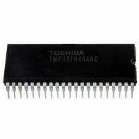
Manufacturer Part Number
TMP86FH46ANG(Z)
Description
IC MCU 8BIT FLASH 16KB 42-SDIP
Manufacturer
Toshiba
Series
TLCS-870/Cr
Datasheet
1.TMP86FH46ANGZ.pdf
(214 pages)
Specifications of TMP86FH46ANG(Z)
Core Processor
870/C
Core Size
8-Bit
Speed
16MHz
Connectivity
SIO, UART/USART
Peripherals
LED, PWM, WDT
Number Of I /o
33
Program Memory Size
16KB (16K x 8)
Program Memory Type
FLASH
Ram Size
512 x 8
Voltage - Supply (vcc/vdd)
2.7 V ~ 5.5 V
Data Converters
A/D 8x10b
Oscillator Type
Internal
Operating Temperature
-40°C ~ 85°C
Package / Case
42-SDIP (0.600", 15.24mm)
Processor Series
TLCS-870
Core
870/C
Data Bus Width
8 bit
Data Ram Size
512 B
Interface Type
SIO, UART
Maximum Clock Frequency
16 MHz
Number Of Programmable I/os
33
Number Of Timers
3
Maximum Operating Temperature
+ 85 C
Mounting Style
Through Hole
Development Tools By Supplier
BMSKTOPAS86FH47(AND), BM1040R0A, BMP86A100010A, BMP86A100010B, BMP86A200010B, BMP86A200020A, BMP86A300010A, BMP86A300020A, BMP86A300030A, SW89CN0-ZCC, SW00MN0-ZCC
Minimum Operating Temperature
- 40 C
On-chip Adc
10 bit, 8 Channel
For Use With
BM1401W0A-G - FLASH WRITER ON-BOARD PROGRAMTMP86C909XB - EMULATION CHIP FOR TMP86F SDIP
Lead Free Status / RoHS Status
Lead free / RoHS Compliant
Eeprom Size
-
Lead Free Status / Rohs Status
Details
Other names
TMP86FH46ANGZ


8.2 TimerCounter Control
Timer Register
8.2 TimerCounter Control
TC1DRA
(0011H, 0010H)
TC1DRB
(0013H, 0012H)
TimerCounter 1 Control Register
MPPG1
ACAP1
MCAP1
METT1
TC1CK
(0014H)
TC1CR
TC1M
TC1S
TFF1
(TC1DRA and TC1DRB).
The TimerCounter 1 is controlled by the TimerCounter 1 control register (TC1CR) and two 16-bit timer registers
Note 1: fc: High-frequency clock [Hz], fs: Low-frequency clock [Hz]
Note 2: The timer register consists of two shift registers. A value set in the timer register becomes valid at the rising edge of the
Note 3: To set the mode, source clock, PPG output control and timer F/F control, write to TC1CR1 during TC1S=00. Set the timer
Timer F/F1 control
Auto capture control
Pulse width measure-
ment mode control
External trigger timer
mode control
PPG output control
TC1 start control
TC1 source clock select
[Hz]
TC1 operating mode
select
first source clock pulse that occurs after the upper byte (TC1DRAH and TC1DRBH) is written. Therefore, write the lower
byte and the upper byte in this order (it is recommended to write the register with a 16-bit access instruction). Writing only
the lower byte (TC1DRAL and TC1DRBL) does not enable the setting of the timer register.
F/F1 control until the first timer start after setting the PPG mode.
TFF1
15
7
MPPG1
14
MCAP1
ACAP1
METT1
6
(Initial value: 1111 1111 1111 1111)
(Initial value: 1111 1111 1111 1111)
13
TC1DRAH (0011H)
TC1DRBH (0013H)
5
0:Auto-capture disable
0:Double edge capture
0:Trigger start
0:Continuous pulse generation
00: Stop and counter clear
01: Command start
10: Rising edge start
11: Falling edge start
00: Timer/external trigger timer/event counter mode
01: Window mode
10: Pulse width measurement mode
11: PPG (Programmable pulse generate) output mode
0: Clear
00
01
10
11
12
TC1S
Rising edge count (Event)
Positive logic count (Window)
Falling edge count (Event)
Negative logic count (Window)
11
4
10
(Ex-trigger/Pulse/PPG)
(Ex-trigger/Pulse/PPG)
DV7CK = 0
3
fc/2
fc/2
fc/2
TC1CK
11
7
3
Page 68
9
NORMAL1/2, IDLE1/2 mode
2
8
External clock (TC1 pin input)
1
7
Timer
Read/Write (Write enabled only in the PPG output mode)
TC1M
O
O
–
–
6
1: Set
1:Auto-capture enable
1:Single edge capture
1:Trigger start and stop
1:One-shot
Extrig-
0
ger
O
O
O
DV7CK = 1
–
fs/2
fc/2
fc/2
5
Read/Write
(Initial value: 0000 0000)
3
7
3
Event
TC1DRAL (0010H)
TC1DRBL (0012H)
O
O
O
–
Read/Write
4
Win-
dow
O
O
O
–
3
Divider
Pulse
DV9
DV5
DV1
TMP86FH46ANG
O
O
O
–
2
SLEEP
SLOW,
mode
PPG
fs/2
O
O
O
O
–
–
1
3
R/W
R/W
R/W
R/W
R/W
0
Related parts for TMP86FH46ANG(Z)
Image
Part Number
Description
Manufacturer
Datasheet
Request
R

Part Number:
Description:
Toshiba Semiconductor [TOSHIBA IGBT Module Silicon N Channel IGBT]
Manufacturer:
TOSHIBA Semiconductor CORPORATION
Datasheet:
Part Number:
Description:
TOSHIBA GTR MODULE SILICON NPN TRIPLE DIFFUSED TYPE
Manufacturer:
TOSHIBA Semiconductor CORPORATION
Datasheet:
Part Number:
Description:
TOSHIBA GTR Module Silicon N Channel IGBT
Manufacturer:
TOSHIBA Semiconductor CORPORATION
Datasheet:
Part Number:
Description:
TOSHIBA Intelligent Power Module Silicon N Channel IGBT
Manufacturer:
TOSHIBA Semiconductor CORPORATION
Datasheet:
Part Number:
Description:
TOSHIBA INTELLIGENT POWER MODULE SILICON N CHANNEL LGBT
Manufacturer:
TOSHIBA Semiconductor CORPORATION
Datasheet:
Part Number:
Description:
TOSHIBA IGBT Module Silicon N Channel IGBT
Manufacturer:
TOSHIBA Semiconductor CORPORATION
Datasheet:
Part Number:
Description:
TOSHIBA GTR MODULE SILICON N−CHANNEL IGBT
Manufacturer:
TOSHIBA Semiconductor CORPORATION
Datasheet:
Part Number:
Description:
TOSHIBA Intelligent Power Module Silicon N Channel IGBT
Manufacturer:
TOSHIBA Semiconductor CORPORATION
Datasheet:
Part Number:
Description:
TOSHIBA GTR Module Silicon N Channel IGBT
Manufacturer:
TOSHIBA Semiconductor CORPORATION
Datasheet:
Part Number:
Description:
TOSHIBA INTELLIGENT POWER MODULE
Manufacturer:
TOSHIBA Semiconductor CORPORATION
Datasheet:
Part Number:
Description:
TOSHIBA Intelligent Power Module Silicon N Channel IGBT
Manufacturer:
TOSHIBA Semiconductor CORPORATION
Datasheet:
Part Number:
Description:
TOSHIBA Intelligent Power Module Silicon N Channel IGBT
Manufacturer:
TOSHIBA Semiconductor CORPORATION
Datasheet:
Part Number:
Description:
TOSHIBA IGBT Module Silicon N Channel IGBT
Manufacturer:
TOSHIBA Semiconductor CORPORATION
Datasheet:
Part Number:
Description:
TOSHIBA Intelligent Power Module Silicon N Channel IGBT
Manufacturer:
TOSHIBA Semiconductor CORPORATION
Datasheet:
Part Number:
Description:
Toshiba Semiconductor [SILICON N CHANNEL 1GBT]
Manufacturer:
TOSHIBA Semiconductor CORPORATION
Datasheet: