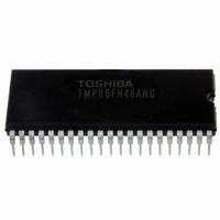
TMP86FH46ANG(Z) Toshiba, TMP86FH46ANG(Z) Datasheet - Page 182

TMP86FH46ANG(Z)
Manufacturer Part Number
TMP86FH46ANG(Z)
Description
IC MCU 8BIT FLASH 16KB 42-SDIP
Manufacturer
Toshiba
Series
TLCS-870/Cr
Datasheet
1.TMP86FH46ANGZ.pdf
(214 pages)
Specifications of TMP86FH46ANG(Z)
Core Processor
870/C
Core Size
8-Bit
Speed
16MHz
Connectivity
SIO, UART/USART
Peripherals
LED, PWM, WDT
Number Of I /o
33
Program Memory Size
16KB (16K x 8)
Program Memory Type
FLASH
Ram Size
512 x 8
Voltage - Supply (vcc/vdd)
2.7 V ~ 5.5 V
Data Converters
A/D 8x10b
Oscillator Type
Internal
Operating Temperature
-40°C ~ 85°C
Package / Case
42-SDIP (0.600", 15.24mm)
Processor Series
TLCS-870
Core
870/C
Data Bus Width
8 bit
Data Ram Size
512 B
Interface Type
SIO, UART
Maximum Clock Frequency
16 MHz
Number Of Programmable I/os
33
Number Of Timers
3
Maximum Operating Temperature
+ 85 C
Mounting Style
Through Hole
Development Tools By Supplier
BMSKTOPAS86FH47(AND), BM1040R0A, BMP86A100010A, BMP86A100010B, BMP86A200010B, BMP86A200020A, BMP86A300010A, BMP86A300020A, BMP86A300030A, SW89CN0-ZCC, SW00MN0-ZCC
Minimum Operating Temperature
- 40 C
On-chip Adc
10 bit, 8 Channel
For Use With
BM1401W0A-G - FLASH WRITER ON-BOARD PROGRAMTMP86C909XB - EMULATION CHIP FOR TMP86F SDIP
Lead Free Status / RoHS Status
Lead free / RoHS Compliant
Eeprom Size
-
Lead Free Status / Rohs Status
Details
Other names
TMP86FH46ANGZ
- Current page: 182 of 214
- Download datasheet (3Mb)
15.6 Operation Mode
Table 15-10 Flash Memory SUM Output Process
BOOT
15.6.4 Flash Memory SUM Output Mode (Operation Command: 90H)
ROM
Note 1: “xxH × 3” indicates that the device enters the halt condition after sending 3 bytes of xxH. For details, refer to " 15.7 Error
Note 2: Refer to " 15.8 Checksum (SUM) ".
1st byte
2nd byte
3rd byte
4th byte
5th byte
6th byte
7th byte
8th byte
9th byte
Table 15-10 shows flash memory SUM output mode process.
Description of the flash memory SUM output mode
Transfer Bytes
Code ".
1. The 1st through 4th bytes of the transmitted and received data contains the same data as in the flash
2. The 5th byte of the received data contains the command data in the flash memory SUM output mode
3. When the 5th byte of the received data contains the operation command data shown in Table 1-6, the
4. The 7th and the 8th bytes contain the upper and lower bits of the checksum, respectively. For how to
5. After sending the checksum, the device waits for the next operation command data.
memory writing mode.
(90H).
device echoes back the value which is the same data in the 6th byte position of the received data (in
this case, 90H). If the 5th byte of the received data does not contain the operation command data, the
device enters the halt condition after transmitting 3 bytes of operation command error code (63H).
calculate the checksum, refer to " 15.8 Checksum (SUM) ".
Matching data (5AH)
-
Baud rate modification data
(See Table 15-4)
-
Operation command data (90H)
-
-
-
(Wait for the next operation com-
mand data)
Transfer Data from External Control-
ler to TMP86FH46ANG
Page 168
9600 bps
9600 bps
9600 bps
9600 bps
Modified baud rate
Modified baud rate
Modified baud rate
Modified baud rate
Modified baud rate
Baud Rate
- (Automatic baud rate adjustment)
OK: Echo back data (5AH)
Error: Nothing transmitted
-
OK: Echo back data
Error: A1H × 3, A3H × 3, 62H × 3 (Note 1)
-
OK: Echo back data (90H)
Error: A1H × 3, A3H × 3, 63H × 3 (Note 1)
OK: SUM (Upper byte) (Note 2)
Error: Nothing transmitted
OK: SUM (Lower byte) (Note 2)
Error: Nothing transmitted
-
Transfer Data from TMP86FH46ANG to
External Controller
TMP86FH46ANG
Related parts for TMP86FH46ANG(Z)
Image
Part Number
Description
Manufacturer
Datasheet
Request
R
Part Number:
Description:
Toshiba Semiconductor [TOSHIBA IGBT Module Silicon N Channel IGBT]
Manufacturer:
TOSHIBA Semiconductor CORPORATION
Datasheet:
Part Number:
Description:
TOSHIBA GTR MODULE SILICON NPN TRIPLE DIFFUSED TYPE
Manufacturer:
TOSHIBA Semiconductor CORPORATION
Datasheet:
Part Number:
Description:
TOSHIBA GTR Module Silicon N Channel IGBT
Manufacturer:
TOSHIBA Semiconductor CORPORATION
Datasheet:
Part Number:
Description:
TOSHIBA Intelligent Power Module Silicon N Channel IGBT
Manufacturer:
TOSHIBA Semiconductor CORPORATION
Datasheet:
Part Number:
Description:
TOSHIBA INTELLIGENT POWER MODULE SILICON N CHANNEL LGBT
Manufacturer:
TOSHIBA Semiconductor CORPORATION
Datasheet:
Part Number:
Description:
TOSHIBA IGBT Module Silicon N Channel IGBT
Manufacturer:
TOSHIBA Semiconductor CORPORATION
Datasheet:
Part Number:
Description:
TOSHIBA GTR MODULE SILICON N−CHANNEL IGBT
Manufacturer:
TOSHIBA Semiconductor CORPORATION
Datasheet:
Part Number:
Description:
TOSHIBA Intelligent Power Module Silicon N Channel IGBT
Manufacturer:
TOSHIBA Semiconductor CORPORATION
Datasheet:
Part Number:
Description:
TOSHIBA GTR Module Silicon N Channel IGBT
Manufacturer:
TOSHIBA Semiconductor CORPORATION
Datasheet:
Part Number:
Description:
TOSHIBA INTELLIGENT POWER MODULE
Manufacturer:
TOSHIBA Semiconductor CORPORATION
Datasheet:
Part Number:
Description:
TOSHIBA Intelligent Power Module Silicon N Channel IGBT
Manufacturer:
TOSHIBA Semiconductor CORPORATION
Datasheet:
Part Number:
Description:
TOSHIBA Intelligent Power Module Silicon N Channel IGBT
Manufacturer:
TOSHIBA Semiconductor CORPORATION
Datasheet:
Part Number:
Description:
TOSHIBA IGBT Module Silicon N Channel IGBT
Manufacturer:
TOSHIBA Semiconductor CORPORATION
Datasheet:
Part Number:
Description:
TOSHIBA Intelligent Power Module Silicon N Channel IGBT
Manufacturer:
TOSHIBA Semiconductor CORPORATION
Datasheet:
Part Number:
Description:
Toshiba Semiconductor [SILICON N CHANNEL 1GBT]
Manufacturer:
TOSHIBA Semiconductor CORPORATION
Datasheet:


